The future of pcb manufacturing
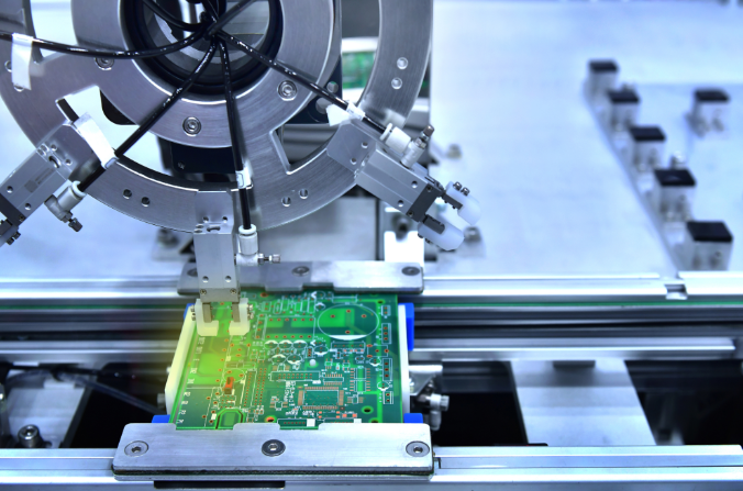
Advances In Automated PCB Assembly
The future of PCB manufacturing is being significantly shaped by advances in automated PCB assembly, a development that promises to revolutionize the industry. As technology continues to evolve, the demand for more efficient, precise, and cost-effective manufacturing processes has never been higher. Automated PCB assembly, which involves the use of sophisticated machinery and software to place and solder components onto printed circuit boards, is at the forefront of meeting these demands.
One of the most notable advancements in this field is the integration of artificial intelligence (AI) and machine learning algorithms.
These technologies enable machines to learn from previous assembly processes, thereby improving accuracy and efficiency over time. For instance, AI can analyze data from past production runs to predict potential issues and optimize the placement of components. This not only reduces the likelihood of errors but also minimizes waste, leading to significant cost savings.
Moreover, the advent of advanced robotics has further enhanced the capabilities of automated PCB assembly.
Modern robotic arms, equipped with high-precision sensors and actuators, can handle even the smallest and most delicate components with remarkable accuracy. This level of precision is particularly crucial as electronic devices continue to shrink in size, necessitating the use of increasingly miniature components. Additionally, these robots can operate continuously without fatigue, ensuring consistent quality and productivity.
In tandem with robotics, the development of sophisticated software tools has also played a pivotal role in advancing automated PCB assembly.
Computer-aided design (CAD) software, for example, allows engineers to create highly detailed and accurate PCB layouts. These layouts can then be directly fed into automated assembly machines, streamlining the entire manufacturing process. Furthermore, simulation software enables manufacturers to test and validate PCB designs virtually before actual production, thereby reducing the risk of costly errors and rework.
Another significant advancement is the implementation of the Internet of Things (IoT) in PCB manufacturing.
IoT devices can collect real-time data from various stages of the assembly process, providing valuable insights into machine performance and production efficiency. This data can be used to identify bottlenecks, predict maintenance needs, and optimize production schedules. Consequently, manufacturers can achieve higher levels of operational efficiency and reduce downtime.
Additionally, the use of advanced materials and innovative manufacturing techniques is also contributing to the evolution of automated PCB assembly.
For example, the development of flexible PCBs, which can be bent and folded without damaging the circuitry, has opened up new possibilities for electronic device design. Automated assembly machines are now capable of handling these flexible materials with ease, enabling the production of more versatile and compact devices.
Furthermore, the push towards sustainability is driving innovations in automated PCB assembly.
Manufacturers are increasingly adopting eco-friendly practices, such as using lead-free solder and recyclable materials. Automated systems can precisely control the amount of solder and other materials used, reducing waste and minimizing the environmental impact of the manufacturing process.
In conclusion, the future of PCB manufacturing is being profoundly influenced by advances in automated PCB assembly. The integration of AI, robotics, sophisticated software tools, IoT, advanced materials, and sustainable practices is transforming the industry, making it more efficient, precise, and environmentally friendly. As these technologies continue to evolve, we can expect even greater innovations that will further enhance the capabilities and potential of automated PCB assembly, ultimately leading to the production of more advanced and reliable electronic devices.
The Role Of AI In PCB Design And Manufacturing
The future of printed circuit board (PCB) manufacturing is poised for a significant transformation, driven by the integration of artificial intelligence (AI) into both design and production processes. As the demand for more complex and efficient electronic devices continues to grow, the traditional methods of PCB manufacturing are increasingly being supplemented and, in some cases, replaced by AI-driven technologies. This shift is not only enhancing the precision and efficiency of PCB production but also opening new avenues for innovation and customization.
To begin with, AI is revolutionizing the design phase of PCB manufacturing.
Traditionally, PCB design has been a meticulous and time-consuming process, requiring extensive expertise and attention to detail. However, AI algorithms are now capable of automating many aspects of this process. For instance, AI can analyze vast amounts of data from previous designs to identify optimal layouts and configurations. This capability allows for the rapid generation of design prototypes, significantly reducing the time required to bring a new product to market. Moreover, AI-driven design tools can predict potential issues such as signal interference or thermal hotspots, enabling designers to address these problems early in the development cycle.
In addition to enhancing the design process, AI is also playing a crucial role in the actual manufacturing of PCBs.
One of the most significant contributions of AI in this area is in quality control. Traditional quality control methods often rely on manual inspection, which can be both time-consuming and prone to human error. AI-powered inspection systems, on the other hand, use machine learning algorithms to detect defects with a high degree of accuracy. These systems can analyze images of PCBs at various stages of production, identifying even the smallest anomalies that might be missed by the human eye. This not only ensures a higher quality product but also reduces waste and rework, leading to more efficient manufacturing processes.
Furthermore, AI is facilitating greater customization in PCB manufacturing.
In the past, producing custom PCBs was often cost-prohibitive due to the need for specialized tooling and lengthy setup times. However, AI-driven manufacturing systems can quickly adapt to new designs and specifications, making it feasible to produce small batches of custom PCBs without significant cost increases. This flexibility is particularly valuable in industries such as aerospace and medical devices, where bespoke solutions are often required.
Another area where AI is making a significant impact is in supply chain management.
The complexity of modern supply chains can make it challenging to ensure the timely delivery of components and materials. AI algorithms can analyze supply chain data to predict potential disruptions and optimize inventory levels, ensuring that manufacturing processes run smoothly. This predictive capability is especially important in the context of global supply chains, where delays or shortages in one region can have a ripple effect on production schedules worldwide.
As we look to the future, the role of AI in PCB design and manufacturing is likely to expand even further.
Advances in machine learning and data analytics will continue to enhance the capabilities of AI systems, enabling even greater levels of automation and precision. Additionally, the integration of AI with other emerging technologies, such as the Internet of Things (IoT) and 5G, will create new opportunities for innovation in PCB design and functionality.
In conclusion, the incorporation of AI into PCB design and manufacturing is transforming the industry, offering significant improvements in efficiency, quality, and customization. As AI technology continues to evolve, its impact on PCB manufacturing will only grow, paving the way for more advanced and sophisticated electronic devices. This ongoing evolution underscores the importance of embracing AI-driven solutions to stay competitive in an increasingly complex and demanding market.
Sustainable Practices In PCB Production
The future of PCB manufacturing is increasingly intertwined with sustainable practices, reflecting a broader shift towards environmental responsibility within the electronics industry. As the demand for electronic devices continues to surge, the need for sustainable production methods has become more pressing. This evolution is driven by both regulatory pressures and a growing awareness among consumers and manufacturers about the environmental impact of traditional PCB production processes.
One of the primary areas of focus in sustainable PCB manufacturing is the reduction of hazardous materials.
Traditional PCB production often involves the use of toxic chemicals such as lead, brominated flame retardants, and volatile organic compounds (VOCs). These substances pose significant environmental and health risks, prompting the industry to seek safer alternatives. For instance, lead-free soldering techniques have gained traction, utilizing materials like tin-silver-copper alloys that offer comparable performance without the associated toxicity. Additionally, the development of halogen-free laminates helps mitigate the release of harmful substances during the manufacturing and disposal phases.
Energy efficiency is another critical aspect of sustainable PCB production.
The manufacturing process is energy-intensive, involving multiple stages such as drilling, plating, and etching, each consuming substantial amounts of electricity. To address this, manufacturers are increasingly adopting energy-efficient technologies and practices. For example, the use of advanced automation and precision machinery can significantly reduce energy consumption by optimizing production processes and minimizing waste. Moreover, integrating renewable energy sources, such as solar or wind power, into manufacturing facilities can further diminish the carbon footprint of PCB production.
Water usage and waste management also play pivotal roles in sustainable PCB manufacturing.
The production process requires large volumes of water, particularly for cleaning and rinsing purposes. To mitigate the environmental impact, manufacturers are implementing closed-loop water systems that recycle and reuse water within the facility, thereby reducing overall consumption. Additionally, advanced filtration and treatment technologies are employed to ensure that any discharged water meets stringent environmental standards, minimizing pollution and protecting local ecosystems.
Material efficiency and waste reduction are equally important in the pursuit of sustainability.
Traditional PCB manufacturing generates significant amounts of waste, including scrap materials and defective boards. To combat this, manufacturers are exploring innovative design and production techniques that maximize material utilization and minimize waste. For instance, additive manufacturing, or 3D printing, allows for the precise deposition of materials, reducing excess and enabling the creation of complex, high-performance PCBs with minimal waste. Furthermore, implementing robust quality control measures throughout the production process helps identify and rectify defects early, reducing the number of discarded boards.
Recycling and end-of-life management are crucial components of a sustainable PCB manufacturing ecosystem.
As electronic devices reach the end of their useful lives, the proper disposal and recycling of PCBs become paramount. Manufacturers are increasingly designing PCBs with recyclability in mind, using materials that can be easily separated and recovered. Additionally, partnerships with specialized recycling facilities ensure that valuable metals and components are extracted and reused, reducing the need for virgin materials and minimizing environmental impact.
In conclusion, the future of PCB manufacturing is being shaped by a concerted effort to adopt sustainable practices.
By reducing hazardous materials, improving energy efficiency, managing water usage and waste, enhancing material efficiency, and prioritizing recycling, the industry is making significant strides towards environmental responsibility. These efforts not only align with regulatory requirements and consumer expectations but also pave the way for a more sustainable and resilient electronics industry. As technology continues to advance, the integration of sustainable practices in PCB production will undoubtedly play a pivotal role in shaping a greener future.
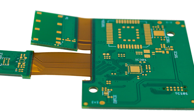
Innovations In Flexible And Wearable PCBs
The future of PCB manufacturing is poised for significant transformation, driven by innovations in flexible and wearable PCBs. As technology continues to evolve, the demand for more adaptable and versatile electronic components has surged, leading to groundbreaking advancements in the field. Flexible PCBs, also known as flex circuits, are at the forefront of this revolution, offering a myriad of benefits over traditional rigid PCBs. These include enhanced durability, reduced weight, and the ability to conform to complex shapes, making them ideal for a wide range of applications.
One of the most notable innovations in flexible PCBs is the development of materials that can withstand extreme conditions while maintaining their functionality.
For instance, polyimide films and liquid crystal polymers are increasingly being used due to their excellent thermal stability and mechanical properties. These materials enable the creation of PCBs that can bend, twist, and fold without compromising their performance, thus opening up new possibilities for electronic device design.
In parallel, the rise of wearable technology has further accelerated the need for flexible PCBs.
Wearable devices, such as smartwatches, fitness trackers, and medical monitoring systems, require electronic components that are not only lightweight and compact but also capable of enduring the rigors of daily use. Flexible PCBs meet these requirements by providing a seamless integration of electronic circuits into fabrics and other flexible substrates. This integration is achieved through advanced manufacturing techniques, such as roll-to-roll processing and additive printing, which allow for the mass production of high-quality flexible circuits at a lower cost.
Moreover, the miniaturization of electronic components has played a crucial role in the advancement of wearable PCBs.
As components become smaller and more efficient, it becomes possible to incorporate more functionality into a single flexible PCB. This trend is particularly evident in the medical field, where wearable devices are being developed to monitor vital signs, deliver medication, and even perform diagnostic tests. These devices rely on flexible PCBs to provide the necessary connectivity and functionality while remaining comfortable and unobtrusive for the wearer.
Another significant innovation in the realm of flexible and wearable PCBs is the advent of stretchable electronics.
Unlike traditional flexible PCBs, which can bend and fold, stretchable PCBs can expand and contract, making them ideal for applications that require a high degree of flexibility and movement. This technology is being explored for use in various fields, including healthcare, sports, and consumer electronics. For example, stretchable PCBs could be used to create smart clothing that monitors physical activity and provides real-time feedback to the wearer.
Furthermore, the integration of flexible and wearable PCBs with other emerging technologies,
such as the Internet of Things (IoT) and artificial intelligence (AI), is set to revolutionize the way we interact with electronic devices. IoT-enabled wearable devices can collect and transmit data to cloud-based platforms, where AI algorithms analyze the information and provide actionable insights. This convergence of technologies promises to enhance the functionality and utility of wearable devices, making them an integral part of our daily lives.
In conclusion, the future of PCB manufacturing is being reshaped by innovations in flexible and wearable PCBs. These advancements are driven by the need for more adaptable, durable, and efficient electronic components that can meet the demands of modern technology. As materials, manufacturing techniques, and component miniaturization continue to improve, flexible and wearable PCBs will play an increasingly vital role in the development of next-generation electronic devices. The potential applications are vast, ranging from healthcare and fitness to consumer electronics and beyond, heralding a new era of technological innovation and integration.


