The Impact of Copper Pour Area in PCB Design: A Comprehensive Analysis
Introduction to Copper Pour in PCB Design
Printed Circuit Board (PCB) design has evolved significantly over the past few decades, with copper pour becoming an essential technique in modern electronic design. Copper pour, also known as copper flooding or copper fill, refers to the process of filling unused areas of a PCB with solid copper that is connected to a net (typically ground). This technique serves multiple purposes in PCB design, from improving manufacturability to enhancing electrical performance.
The copper pour area—the total surface area covered by these copper fills—plays a critical role in determining the board’s overall characteristics. Designers must carefully consider how much of the PCB layers should be covered with copper pour, as this decision impacts thermal management, signal integrity, electromagnetic compatibility (EMC), mechanical strength, and manufacturing yield.
This article will explore the various aspects of copper pour area in PCB design, examining its benefits, potential drawbacks, calculation methods, and optimization strategies across different applications and industries.
Benefits of Proper Copper Pour Area Implementation
Thermal Management Advantages
One of the primary benefits of appropriate copper pour area implementation is improved thermal performance. Copper’s excellent thermal conductivity (approximately 400 W/m·K at room temperature) makes it ideal for heat dissipation in electronic circuits.
The relationship between copper pour area and thermal resistance can be expressed as:
θ = L / (k × A)
Where:
- θ is the thermal resistance (°C/W)
- L is the length of the heat flow path (m)
- k is the thermal conductivity of copper (W/m·°C)
- A is the cross-sectional area (copper pour area in this context)
This equation demonstrates that increasing the copper pour area directly reduces thermal resistance, allowing for more efficient heat spreading across the board. For power electronics applications, where components may generate substantial heat, large copper pour areas (often 70-90% of available space) are typically employed to prevent thermal buildup and ensure reliable operation.
Signal Integrity Improvements
Copper pour area significantly impacts signal integrity, particularly in high-speed digital designs. Properly implemented ground copper pours serve as reference planes for controlled impedance traces and provide return paths for high-frequency signals.
The characteristic impedance of a microstrip trace over a copper pour (ground plane) can be calculated using:
Z₀ = [87 / √(ε_r + 1.41)] × ln[5.98h / (0.8w + t)]
Where:
- Z₀ is the characteristic impedance (Ω)
- ε_r is the dielectric constant of the substrate
- h is the height of the substrate (distance to copper pour)
- w is the width of the trace
- t is the thickness of the trace
This relationship shows how the presence and proximity of copper pour affect impedance control. In multilayer boards, maintaining consistent copper pour areas (typically >80%) on reference planes helps minimize impedance variations and reduces signal reflections.
Electromagnetic Compatibility (EMC) Enhancement
Copper pour area plays a crucial role in EMC performance by:
- Providing shielding against electromagnetic interference (EMI)
- Reducing loop areas that can act as antennas
- Lowering ground impedance, which decreases common-mode noise
The shielding effectiveness (SE) of a copper pour can be approximated by:
SE(dB) = 20 log₁₀(π × f × μ × σ × A / 2)
Where:
- f is the frequency (Hz)
- μ is the permeability of copper (H/m)
- σ is the conductivity of copper (S/m)
- A is the area of the copper pour (m²)
This equation indicates that larger copper pour areas provide better high-frequency shielding. For sensitive analog circuits or high-speed digital designs, maintaining continuous copper pours (with minimal splits) of at least 60-70% coverage per layer is often recommended for optimal EMC performance.
Calculating Optimal Copper Pour Area
Copper Area Percentage Calculations
The copper pour area percentage is typically calculated as:
Copper Area % = (Total Copper Pour Area / Total Available Board Area) × 100
However, this simple calculation doesn’t account for several critical factors:
- Copper distribution uniformity
- Proximity to board edges
- Relationship to component density
- Layer-specific requirements
More sophisticated calculations might consider:
- Copper density by board quadrant to ensure even distribution
- Copper-to-edge clearance requirements (typically 0.5-1mm for manufacturing)
- Component shadow areas where copper may need to be removed
Current Carrying Capacity Considerations
When using copper pours for power distribution (rather than just ground), the current carrying capacity must be calculated. The IPC-2152 standard provides guidelines for determining the required copper area based on current requirements:
A = (I / (k × ΔT^0.44))^(1/0.725)
Where:
- A is the cross-sectional area (mils²)
- I is the current (A)
- ΔT is the temperature rise (°C)
- k is a constant (0.048 for external layers, 0.024 for internal layers)
This calculation helps determine the minimum copper pour area needed for power nets to prevent excessive temperature rise.

Thermal Expansion Considerations
The coefficient of thermal expansion (CTE) mismatch between copper (17 ppm/°C) and common PCB substrates (typically 12-18 ppm/°C in x-y axes) must be considered, especially for large copper pour areas. The relative area can be calculated as:
CTE_diff = |CTE_copper – CTE_substrate| × ΔT × Area_ratio
Where:
- Area_ratio = Copper_area / Total_board_area
For boards with >50% copper pour area, this calculation becomes particularly important to predict potential warping or delamination issues during thermal cycling.
Copper Pour Area in Different PCB Applications
High-Speed Digital PCBs
In high-speed digital designs (e.g., servers, networking equipment), copper pour area typically covers 70-90% of each layer. Key considerations include:
- Maintaining uninterrupted reference planes for impedance control
- Providing low-impedance return paths for high-frequency signals
- Minimizing via-induced discontinuities in copper pours
The high copper area percentage helps maintain signal integrity at multi-gigabit data rates by reducing ground bounce and crosstalk.
RF/Microwave PCBs
RF designs require careful copper pour area management:
- Often use 100% copper pour (entire layer as ground) for microstrip designs
- May employ strategic copper removal (20-50% area) in certain regions to control dielectric constant
- Require precise calculation of copper area around transmission lines to maintain impedance
The skin effect becomes significant at RF frequencies, making surface copper area particularly important:
δ = √(ρ / (π × f × μ))
Where δ is the skin depth (m), showing that current flows primarily in the outer layer of copper at high frequencies.
Power Electronics PCBs
Power electronics designs prioritize thermal performance and current handling:
- Typically feature 60-80% copper pour area on power layers
- May use thick copper (2-8 oz) with correspondingly larger area requirements
- Often employ copper coins or inlays in high-current areas
The copper area must be sufficient to handle peak currents without excessive temperature rise, as calculated by the IPC-2152 formulas mentioned earlier.
Copper Pour Area and Manufacturing Considerations
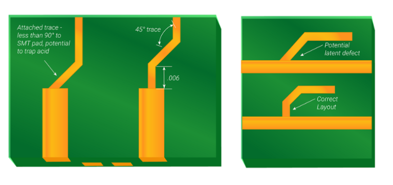
Etching Process Implications
The copper pour area affects the etching process in several ways:
- Etch Factor: Higher copper area percentages (especially >70%) require longer etch times
- Copper Thickness: Thicker copper requires more etch compensation
- Uniformity: Large continuous copper areas can lead to uneven etching
Manufacturers often recommend:
- Minimum 10-15% copper removal (85-90% max copper area)
- Adding thieving (dummy copper features) in sparse areas
- Maintaining copper balance across layers (within 20-30% area difference)
Layer-to-Layer Registration
High copper pour area designs (particularly >80%) present registration challenges:
- Copper’s thermal expansion can affect alignment during lamination
- Large copper areas may cause layer shifting during processing
- Requires precise tooling and material selection
Designs should maintain:
- Adequate clearance around tooling holes
- Balanced copper distribution
- Consideration of material CTE properties
Warpage Control
The relationship between copper pour area and warpage can be estimated by:
Warpage ∝ (CTE_mismatch) × (Copper_area_imbalance) × ΔT × L²
Where L is the board dimension. To minimize warpage:
- Maintain copper area balance within 20% between opposite sides
- Use symmetrical stackups
- Consider copper thieving in sparse areas
Advanced Copper Pour Area Techniques
Segmented Copper Pours
Modern designs often employ segmented copper pours for:
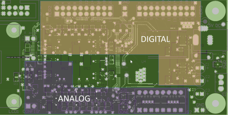
- Mixed-signal isolation (separate analog and digital ground areas)
- Thermal zone control
- Voltage island implementation
Segmentation strategies must consider:
- Proper bridging at single-point connections
- Maintaining adequate copper area in each segment
- Avoiding antenna effects from isolated copper islands
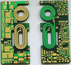
Copper Pour in HDI Designs
High Density Interconnect (HDI) PCBs present unique copper pour challenges:
- Microvia-in-pad techniques may require local copper removal
- Tight spacing limits continuous copper area (often 50-70%)
- Requires precise calculation of remaining copper for current capacity
3D Copper Area Optimization
Advanced designs consider copper area in three dimensions:
- Vertical thermal vias connect copper areas across layers
- Copper volume calculations replace simple area calculations
- 3D current density simulations inform copper distribution
Conclusion and Best Practices
Optimizing copper pour area in PCB design requires balancing multiple competing factors. Based on the analysis presented, these best practices emerge:
- General Guidelines:
- Aim for 60-80% copper area on signal layers
- Maintain 70-90% on ground/power planes
- Ensure layer-to-layer balance within 20%
- High-Speed Designs:
- Prioritize continuous reference planes (>85% copper)
- Minimize splits in return paths
- Use calculated clearance around high-speed traces
- Power Electronics:
- Size copper area based on current requirements
- Consider thick copper options for high-current paths
- Implement thermal relief patterns carefully
- Manufacturing Considerations:
- Maintain minimum 0.2mm copper-to-edge clearance
- Avoid isolated copper islands (<2mm²)
- Balance copper distribution across the panel
- Advanced Techniques:
- Implement segmented pours for mixed-signal designs
- Use 3D analysis for multilayer copper optimization
- Consider thermal expansion effects in large boards
The optimal copper pour area ultimately depends on the specific application, performance requirements, and manufacturing constraints. By understanding the underlying principles and relationships presented in this article, designers can make informed decisions about copper pour implementation to create reliable, high-performance PCBs.
Future trends in copper pour area management may include:
- AI-driven copper area optimization
- Dynamic copper pour adjustment based on real-time thermal data
- Advanced materials with tailored CTE for high-copper-area designs
As PCB technology continues to advance, the precise control and optimization of copper pour area will remain a critical factor in electronic design success.
Introduction to Copper Pour in PCB Design
Printed Circuit Board (PCB) design has evolved significantly over the past few decades, with copper pour becoming an essential technique in modern electronic design. Copper pour, also known as copper flooding or copper fill, refers to the process of filling unused areas of a PCB with solid copper that is connected to a net (typically ground). This technique serves multiple purposes in PCB design, from improving manufacturability to enhancing electrical performance.
The copper pour area—the total surface area covered by these copper fills—plays a critical role in determining the board’s overall characteristics. Designers must carefully consider how much of the PCB layers should be covered with copper pour, as this decision impacts thermal management, signal integrity, electromagnetic compatibility (EMC), mechanical strength, and manufacturing yield.
This article will explore the various aspects of copper pour area in PCB design, examining its benefits, potential drawbacks, calculation methods, and optimization strategies across different applications and industries.
Benefits of Proper Copper Pour Area Implementation
Thermal Management Advantages
One of the primary benefits of appropriate copper pour area implementation is improved thermal performance. Copper’s excellent thermal conductivity (approximately 400 W/m·K at room temperature) makes it ideal for heat dissipation in electronic circuits.
The relationship between copper pour area and thermal resistance can be expressed as:
θ = L / (k × A)
Where:
- θ is the thermal resistance (°C/W)
- L is the length of the heat flow path (m)
- k is the thermal conductivity of copper (W/m·°C)
- A is the cross-sectional area (copper pour area in this context)
This equation demonstrates that increasing the copper pour area directly reduces thermal resistance, allowing for more efficient heat spreading across the board. For power electronics applications, where components may generate substantial heat, large copper pour areas (often 70-90% of available space) are typically employed to prevent thermal buildup and ensure reliable operation.
Signal Integrity Improvements
Copper pour area significantly impacts signal integrity, particularly in high-speed digital designs. Properly implemented ground copper pours serve as reference planes for controlled impedance traces and provide return paths for high-frequency signals.
The characteristic impedance of a microstrip trace over a copper pour (ground plane) can be calculated using:
Z₀ = [87 / √(ε_r + 1.41)] × ln[5.98h / (0.8w + t)]
Where:
- Z₀ is the characteristic impedance (Ω)
- ε_r is the dielectric constant of the substrate
- h is the height of the substrate (distance to copper pour)
- w is the width of the trace
- t is the thickness of the trace
This relationship shows how the presence and proximity of copper pour affect impedance control. In multilayer boards, maintaining consistent copper pour areas (typically >80%) on reference planes helps minimize impedance variations and reduces signal reflections.
Electromagnetic Compatibility (EMC) Enhancement
Copper pour area plays a crucial role in EMC performance by:
- Providing shielding against electromagnetic interference (EMI)
- Reducing loop areas that can act as antennas
- Lowering ground impedance, which decreases common-mode noise
The shielding effectiveness (SE) of a copper pour can be approximated by:
SE(dB) = 20 log₁₀(π × f × μ × σ × A / 2)
Where:
- f is the frequency (Hz)
- μ is the permeability of copper (H/m)
- σ is the conductivity of copper (S/m)
- A is the area of the copper pour (m²)
This equation indicates that larger copper pour areas provide better high-frequency shielding. For sensitive analog circuits or high-speed digital designs, maintaining continuous copper pours (with minimal splits) of at least 60-70% coverage per layer is often recommended for optimal EMC performance.
Calculating Optimal Copper Pour Area
Copper Area Percentage Calculations
The copper pour area percentage is typically calculated as:
Copper Area % = (Total Copper Pour Area / Total Available Board Area) × 100
However, this simple calculation doesn’t account for several critical factors:
- Copper distribution uniformity
- Proximity to board edges
- Relationship to component density
- Layer-specific requirements
More sophisticated calculations might consider:
- Copper density by board quadrant to ensure even distribution
- Copper-to-edge clearance requirements (typically 0.5-1mm for manufacturing)
- Component shadow areas where copper may need to be removed
Current Carrying Capacity Considerations
When using copper pours for power distribution (rather than just ground), the current carrying capacity must be calculated. The IPC-2152 standard provides guidelines for determining the required copper area based on current requirements:
A = (I / (k × ΔT^0.44))^(1/0.725)
Where:
- A is the cross-sectional area (mils²)
- I is the current (A)
- ΔT is the temperature rise (°C)
- k is a constant (0.048 for external layers, 0.024 for internal layers)
This calculation helps determine the minimum copper pour area needed for power nets to prevent excessive temperature rise.
Thermal Expansion Considerations
The coefficient of thermal expansion (CTE) mismatch between copper (17 ppm/°C) and common PCB substrates (typically 12-18 ppm/°C in x-y axes) must be considered, especially for large copper pour areas. The relative area can be calculated as:
CTE_diff = |CTE_copper – CTE_substrate| × ΔT × Area_ratio
Where:
- Area_ratio = Copper_area / Total_board_area
For boards with >50% copper pour area, this calculation becomes particularly important to predict potential warping or delamination issues during thermal cycling.
Copper Pour Area in Different PCB Applications
High-Speed Digital PCBs
In high-speed digital designs (e.g., servers, networking equipment), copper pour area typically covers 70-90% of each layer. Key considerations include:
- Maintaining uninterrupted reference planes for impedance control
- Providing low-impedance return paths for high-frequency signals
- Minimizing via-induced discontinuities in copper pours
The high copper area percentage helps maintain signal integrity at multi-gigabit data rates by reducing ground bounce and crosstalk.
RF/Microwave PCBs
RF designs require careful copper pour area management:
- Often use 100% copper pour (entire layer as ground) for microstrip designs
- May employ strategic copper removal (20-50% area) in certain regions to control dielectric constant
- Require precise calculation of copper area around transmission lines to maintain impedance
The skin effect becomes significant at RF frequencies, making surface copper area particularly important:
δ = √(ρ / (π × f × μ))
Where δ is the skin depth (m), showing that current flows primarily in the outer layer of copper at high frequencies.
Power Electronics PCBs
Power electronics designs prioritize thermal performance and current handling:
- Typically feature 60-80% copper pour area on power layers
- May use thick copper (2-8 oz) with correspondingly larger area requirements
- Often employ copper coins or inlays in high-current areas
The copper area must be sufficient to handle peak currents without excessive temperature rise, as calculated by the IPC-2152 formulas mentioned earlier.
Copper Pour Area and Manufacturing Considerations
Etching Process Implications
The copper pour area affects the etching process in several ways:
- Etch Factor: Higher copper area percentages (especially >70%) require longer etch times
- Copper Thickness: Thicker copper requires more etch compensation
- Uniformity: Large continuous copper areas can lead to uneven etching
Manufacturers often recommend:
- Minimum 10-15% copper removal (85-90% max copper area)
- Adding thieving (dummy copper features) in sparse areas
- Maintaining copper balance across layers (within 20-30% area difference)
Layer-to-Layer Registration
High copper pour area designs (particularly >80%) present registration challenges:
- Copper’s thermal expansion can affect alignment during lamination
- Large copper areas may cause layer shifting during processing
- Requires precise tooling and material selection
Designs should maintain:
- Adequate clearance around tooling holes
- Balanced copper distribution
- Consideration of material CTE properties
Warpage Control
The relationship between copper pour area and warpage can be estimated by:
Warpage ∝ (CTE_mismatch) × (Copper_area_imbalance) × ΔT × L²
Where L is the board dimension. To minimize warpage:
- Maintain copper area balance within 20% between opposite sides
- Use symmetrical stackups
- Consider copper thieving in sparse areas
Advanced Copper Pour Area Techniques
Segmented Copper Pours
Modern designs often employ segmented copper pours for:
- Mixed-signal isolation (separate analog and digital ground areas)
- Thermal zone control
- Voltage island implementation
Segmentation strategies must consider:
- Proper bridging at single-point connections
- Maintaining adequate copper area in each segment
- Avoiding antenna effects from isolated copper islands
Copper Pour in HDI Designs
High Density Interconnect (HDI) PCBs present unique copper pour challenges:
- Microvia-in-pad techniques may require local copper removal
- Tight spacing limits continuous copper area (often 50-70%)
- Requires precise calculation of remaining copper for current capacity
3D Copper Area Optimization
Advanced designs consider copper area in three dimensions:
- Vertical thermal vias connect copper areas across layers
- Copper volume calculations replace simple area calculations
- 3D current density simulations inform copper distribution
Conclusion and Best Practices
Optimizing copper pour area in PCB design requires balancing multiple competing factors. Based on the analysis presented, these best practices emerge:
- General Guidelines:
- Aim for 60-80% copper area on signal layers
- Maintain 70-90% on ground/power planes
- Ensure layer-to-layer balance within 20%
- High-Speed Designs:
- Prioritize continuous reference planes (>85% copper)
- Minimize splits in return paths
- Use calculated clearance around high-speed traces
- Power Electronics:
- Size copper area based on current requirements
- Consider thick copper options for high-current paths
- Implement thermal relief patterns carefully
- Manufacturing Considerations:
- Maintain minimum 0.2mm copper-to-edge clearance
- Avoid isolated copper islands (<2mm²)
- Balance copper distribution across the panel
- Advanced Techniques:
- Implement segmented pours for mixed-signal designs
- Use 3D analysis for multilayer copper optimization
- Consider thermal expansion effects in large boards
The optimal copper pour area ultimately depends on the specific application, performance requirements, and manufacturing constraints. By understanding the underlying principles and relationships presented in this article, designers can make informed decisions about copper pour implementation to create reliable, high-performance PCBs.
Future trends in copper pour area management may include:
- AI-driven copper area optimization
- Dynamic copper pour adjustment based on real-time thermal data
- Advanced materials with tailored CTE for high-copper-area designs
As PCB technology continues to advance, the precise control and optimization of copper pour area will remain a critical factor in electronic design success.