The impact of integrated passive components on the development of PCB technology
The impact of integrated passive components on the development of PCB technology
Integrated passive component technology can integrate multiple electronic functions, with the advantages of miniaturization and improved system performance, to replace bulky discrete passive components. This article mainly introduces the development of integrated passive component technology, as well as the use of IPD thin film technology to realize the processing of capacitors, resistors and inductors, and explores the impact of IPD on the development of PCB technology.
1 Introduction
With the development of electronic technology, after semiconductors entered the nano process from micron process, the integration of active electronic components has been greatly improved, and the demand for passive components that match active components has increased significantly. The market development trend of electronic products is to be thin, light and short, so the improvement of semiconductor process capabilities has greatly increased the number of active components in the same volume. In addition to the significant increase in the number of supporting passive components, more space is also needed to place these passive components, so the size of the overall packaged device will inevitably increase, which is very different from the development trend of the market. From a cost perspective, the total cost is proportional to the number of passive components. Therefore, under the premise of using a large number of passive components, how to reduce the cost and space of passive components, and even improve the performance of passive components, is one of the most important issues at present.
IPD (Integrated Passive Devices) technology can integrate a variety of electronic functions, such as sensors, RF transceivers, micro-electromechanical systems MEMS, power amplifiers, power management units and digital processors, etc., to provide compact integrated passive device IPD products with the advantages of miniaturization and improved system performance. Therefore, whether it is to reduce the size and weight of the entire product or to increase functions within the existing product volume, integrated passive component technology can play a big role.
In the past few years, IPD technology has become an important implementation method of system-level packaging (SiP). IPD technology will pave the way for integrated multifunctionality that “surpasses Moore’s Law”; at the same time, PCB processing can introduce IPD technology, and through the integration advantages of IPD technology, it can bridge the widening gap between packaging technology and PCB technology.
IPD integrated passive component technology has developed from the initial commercial technology to the current replacement of discrete passive components, and has grown steadily driven by industries such as ESD/EMI, RF, high-brightness LEDs and digital hybrid circuits.
2 Introduction to thin-film IPD technology
IPD technology can be divided into thick film process and thin film process according to process technology. Among them, thick film process technology includes low-temperature co-fired ceramics LTCC (Low Temperature Co-fired Ceramics) technology using ceramic as a substrate and embedded passive components (Embedded Passives) technology based on HDI high-density interconnection PCB printed circuit board; while thin-film IPD technology uses commonly used semiconductor technology to make circuits and capacitors, resistors and inductors.
LTCC technology uses ceramic materials as a substrate to make capacitors. Passive components such as resistors are embedded in ceramic substrates and sintered to form integrated ceramic components, which can greatly reduce the space of components. However, as the number of layers increases, the difficulty and cost of production increase. Therefore, LTCC components are mostly for circuits with a specific function; HDI embedded component PCB technology is usually used in digital systems. In such systems, it is only suitable for distributed soldered capacitors and medium and low precision resistors. As the size of components decreases, SMT equipment is not easy to handle small components. Although embedded printed circuit board technology is the most mature, the product characteristics are poor and the tolerance cannot be accurately grasped. Because the components are buried in the multi-layer board, it is difficult to replace or repair and adjust after problems occur. Compared with LTCC technology and PCB embedded component technology, thin film IPD technology of integrated circuits has the advantages of high precision, high repeatability, small size, high reliability and low cost. It is bound to become the mainstream of IPD in the future. This article will mainly introduce thin film IPD technology.
3 Current Development of Thin Film Integrated Passive Component Technology
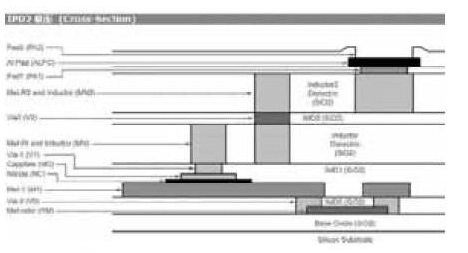
Thin film IPD technology uses thin film processes such as exposure, development, coating, diffusion, and etching. A cross-sectional diagram of a representative thin film integrated passive process is shown in Figure 1. This process can produce various resistors, capacitors, and inductors, as well as low-inductance ground planes and transmission line traces connecting passive components. The thin film structure is manufactured on a suitable carrier substrate material. The process must not only meet the required component performance and precision indicators, but also cannot be complicated, requiring a small number of masks (usually 6 to 10 sheets). Each passive component usually occupies less than 1 mm2 of area, so that it can compete with discrete components of surface mount technology in terms of area and cost.
Based on the existing IPD structure, the development manufacturers are introduced as follows:
(1) Telephus
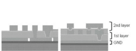
The IPD developed by Telephus uses a thick copper process, which can improve the performance of lines with only passive components. To reduce costs and size, such as filters and dividers, thick copper metal layers (10 mm) and silicon insulating surfaces enable wireless communication systems and integrated RF modules to have high performance, while low dielectric constant materials are suitable for reducing parasitic capacitance between metal layers. Its IPD structure is shown in Figure 2.
(2) IMEC
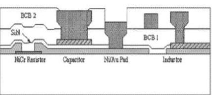
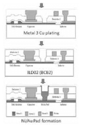
IMEC’s thin film technology also uses electroplated copper as the connection line, BCB as the dielectric layer, and Ni/Au layer as the final connection surface metal, using up to 4 layers of metal layers. Its IPD structure is shown in Figure 3.
(3) Dai Nippon
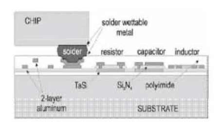
The IPD resistors developed by Dai Nippon are mainly Ti/Cr, and the capacitors are made of Ta2O5 by anodizing. The inductor is designed with microstrip lines and spiral inductors, and the lines are mainly copper. Its IPD structure is shown in Figure 4.
(4) SyChip
The IPD developed by SyChip uses TaSi as the resistor material, Si3N4 as the dielectric material of the capacitor, Al as the upper electrode, TaSi as the lower electrode, and aluminum as the inductor and line material. Its IPD structure is shown in Figure 5.
Some companies are using MEMS technology to develop IPD, such as PHS MEMS. According to the company, the method of manufacturing MEMS components basically comes from the IC industry. At the same time, some established companies, while developing related technologies, also acquire markets and technologies through acquisitions. For example, Murata acquired SyChip, hoping to expand its share in the RF application market through this acquisition.
4 Structure and process of thin film integrated passive component technology
The biggest difference between thin film process and thick film process is the film thickness produced. Generally speaking, the so-called thick film thickness is more than 5μm ~ 10μm, while the film thickness produced by thin film process is about 0.01μm ~ 1μm.
If thin film processes are used to form resistors, capacitors, and inductors at the same time, different processes and materials are required to make them.
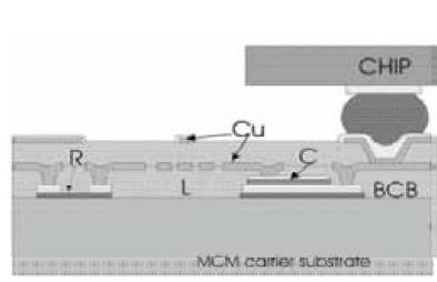
Thin film technology is applied in semiconductor integrated circuit processes, and the technology development is quite mature. Therefore, when performing process integration, you only need to pay attention to the compatibility of materials between different components to achieve process design.
Overall, thin film IPD integrated passive components can be made on different substrates due to different product applications, and the substrate can be selected from silicon wafers. Alumina ceramic substrates, glass substrates, and thin film IPD integrated passive component technology can integrate thin film resistors, capacitors, and inductors. Its process technology development includes: lithography processing technology, thin film deposition processing technology, etching processing technology, electroplating processing technology, and electrodeless electroplating processing technology. The entire processing flow is shown in Figure 6. In addition to the integration of passive components, the process of active components can also be combined on silicon wafers to integrate passive components with active component circuits to meet multifunctional needs. The following is a brief introduction to the processing of thin film resistors, capacitors, and inductors.
(1) Thin film resistor processing
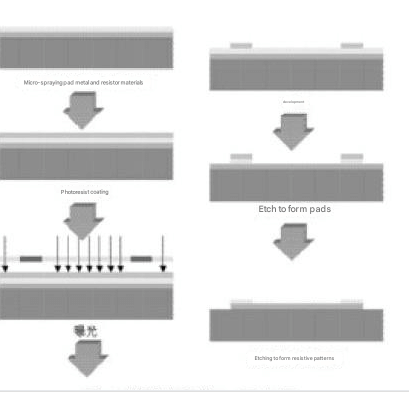
Thin film resistors are usually made by sputtering process. The resistor material is electroplated on the insulating substrate, and then the photoresist and etching technology are used to process the resistor pattern to obtain the designed resistance value. The process diagram is shown in Figure 7.
In the application of materials, it is necessary to consider the TCR of the resistor material, that is, the resistance change rate at different temperatures. Thin film resistors are formed by vacuum evaporation, sputtering, thermal decomposition and electroplating, and the commonly used resistor materials include single component metal, alloy and metal ceramic.
(2) Thin film capacitor processing
Because MIS (Metal-Insulator-Semiconductor) thin film capacitors use semiconductors as the bottom electrode, the capacitor itself has parasitic resistance, which reduces the resonant frequency of the component and cannot be used for frequencies above 200 MHz. Therefore, for high-frequency applications, MIM (Metal-Insulator-Metal) thin film capacitors must be selected. MIM capacitors can reduce the parasitic resistance value and thus increase the resonant frequency of the component. The resonant frequency depends on the self-resonance frequency of the dielectric material. Like thin film resistors, thin film capacitors need to consider the capacitance change rate, and the dielectric constant also needs to be considered.
In addition, the surface roughness Ra of the substrate needs to be noted
5 The impact of IPD technology on the development of PCB technology
With the advancement of technology, PCB printed circuit boards are developing towards higher precision and higher density, and are gradually highly integrated with the IC packaging field. Passive component integration is in line with the development trend of today’s electronic systems. IPD technology has become an important implementation method of system-level packaging (SiP).
IPD integrated passive component technology has the advantages of high wiring density, small size, light weight; high integration, and can bury passive devices such as resistors, inductors, capacitors and active chips; good high-frequency characteristics, can be used in microwave and millimeter wave fields, etc. Applying thin-film IPD integrated passive component technology to PCB processing can achieve the goals of saving packaging area, improving signal transmission performance, reducing costs, and improving reliability; through the integration advantages of IPD technology, bridging the ever-widening gap between packaging technology and PCB technology, it can effectively reduce the volume and weight of electronic equipment and systems, and has broad market prospects.
When applying PCB processing to IPD integrated passive components, high-thermal conductive metals, diamonds, ceramics or aluminum-silicon carbide composite materials can be selected as substrates to manufacture high-density and high-power multi-layer circuit substrates. At the same time, the process improvement, material property improvement and low cost of IPD passive integrated PCB substrates should be strengthened, and their application in microwave communications, high-density integration and high-power fields should be accelerated.
6 Conclusion
Thin-film IPD integrated passive component technology can integrate multiple electronic functions, has the advantages of miniaturization and improved system performance, and can replace bulky discrete passive components. At the same time, IPD technology can be introduced into PCB processing. Through the integration advantages of IPD technology, the widening gap between packaging technology and PCB technology can be bridged.
The rapid development of thin-film IPD integrated passive component technology has enabled passive integration technology to enter the practical and industrialization stage. The new generation of passive components and related integration technologies will be widely used in the electronics industry in various fields such as aerospace, military industry, medical treatment, industrial control and communication. Therefore, the development of IPD technology is of great significance both to the development of the enterprise itself and to enhance the competitiveness of the domestic industry.


