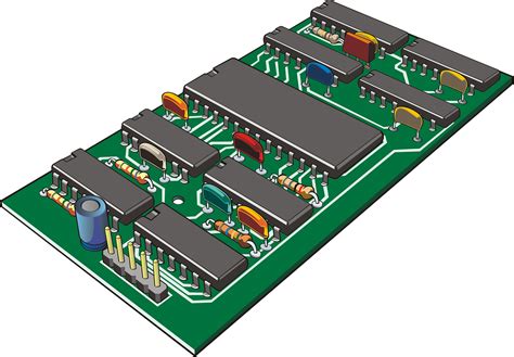
The Impact of IoT Development on PCB Industry
Since the birth of the dot-com bubble, the Internet of Things (IoT) has developed into the most important movement with monikers such as “the fourth industrial revolution” or “the infrastructure of the information society”. The impact of IoT has been deeply integrated into the framework of technology and daily life.
Many consumers may not realize that IoT PCBs are at the forefront of IoT’s penetration into daily technology, and likewise, IoT plays an integral role in the transformation of PCB design and manufacturing. As the demand for more IoT devices grows, understanding the interconnection between IoT and Flex and HDI PCBs becomes increasingly important for PCB designers.
What is IoT?
IoT is the crossover between the physical and digital worlds brought about by the creation of devices other than PCs that connect to IP networks. Smartphones may be the most prominent example of IoT, but more recently, the development of applications for controlling home appliances and utilities, or the introduction of wearable technology and vehicles with data accessibility have proven that the potential of IoT is limitless.
Consumer electronics may be the first innovation that comes to mind, but the manufacturing, transportation, and healthcare industries are even ahead of personal cars and electronics in the command of the IoT revolution. As a result, these large industries require innovative PCB designs that offer flexibility and high-speed connectivity to streamline processes around the world.
PCB Applications Driven by the Internet of Things
PCBs are at the center of enabling electronic devices to deliver IoT capabilities found in smart home applications or mobile screens in car dashboards, but IoT is also influencing PCB design and applications to meet the growing demand for new ways to use the Internet, including:
- Sensors and cameras in cars and home utilities that provide new levels of efficiency, convenience, and safety.
- Fitness trackers whose data can be analyzed remotely.
- Light bulbs that change color to create customized moods for different rooms, which can be managed from tablets or even smaller smart devices.
- Grid layouts in shopping malls or amusement parks that monitor consumer routes to provide customized sales opportunities for retailers and customers.
Whether it’s monitoring train arrival times and maintenance needs to create reliable shipping schedules, or tracking real-time traffic via satellite to optimize personal GPS navigation to car dashboards, PCBs make all new ideas possible. In medical devices and wearables, without changing the design of PCB form factors to provide flexibility to fit any shape or high density to fill small spaces with high-power functions, the Internet of Things will not be as feasible as it is now, nor will it be as promising in the future.
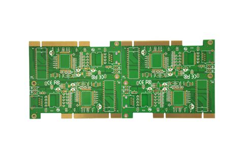
IoT Opportunities with Flex and HDI PCBs
Gone are the days when the shape and size of a computer was determined by the structure of its necessary internal components. Now, the entire industry is looking to create an optimal IoT product that functions the same regardless of the form factor. It has become essential to reimagine the internal circuitry to reflect this change in approach.
To achieve new forms of functionality and sustainability, printed electronics technology has led the way in complex manufacturing. Flexible PCBs and high-density interconnect (HDI) PCBs offer design freedom to meet the requirements of high power in increasingly tight board spaces, are suitable for harsh environments and constant device stress, and have high copper tensile strength.
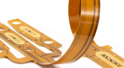
Advantages of Flexible Printed Circuit Boards and IoT
The introduction of flexible PCBs can greatly reduce design constraints that you may encounter with more rigid traditional PCBs. Thanks to the beneficial features of flexible PCBs, flexible board structures not only pave the way for revolutionizing the forms and shapes our electronic products can take, but also reduce costs and errors. Some of the best attributes that make flexible PCBs suitable for IoT designs include:
l Smaller size: The bulk of rigid PCBs limit design freedom but tend to take up more space within the product. By reducing the volume, flexible PCBs allow components such as microphones, satellites, and batteries to all fit into a small package without compromising performance. Thin components also allow flexible PCBs to support denser circuits.
l Lighter weight: With less space, weight can also be saved by up to 95%. Lightweight internal component options allow IoT devices to have more versatility in a variety of uses and environments, such as delicate surgical equipment or wearable hearing aids.
l Higher resistance: Flexible PCB materials offer higher durability, improving resistance to stress caused by shock or vibration. In industrial environments, where the use of IoT PCBs is expanding, flexible PCBs can withstand harsher conditions. Similarly, for devices such as fitness trackers, flexible PCBs can resist errors caused by regular exercise, body heat, or moisture.
lClearer Routing: Flexible PCBs eliminate mechanical connectors, which simplifies the wiring approach. This simplified routing becomes a valuable asset when imagining how the complexity of the mechanical structure under the hood of a car can be improved with IoT capabilities, for example.
Flexible PCBs’ flexible materials used as circuit connectors open up endless possibilities for mobile devices and movable parts, making them an incredible tool for a wide range of IoT endeavors. If you and your company are about to launch a novel flexible printed circuit board, be sure to contact MCL for answers on the best flexible PCB materials for your industry and manufacturing quotes.
To accommodate the smaller space that flexible PCBs may offer, HDI PCBs are here to provide the highest board density for optimal circuit performance.
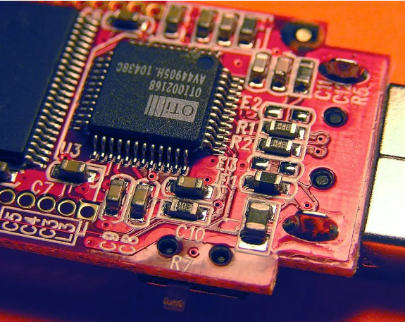
Benefits of High Density Interconnect PCBs and IoT
As the leader in the small package designs we see in personal electronics today, high-density interconnect (HDI) PCBs are an essential tool. When facing the big picture of IoT, designers and manufacturers alike need to consider the advantages of these boards, including their speed and reliability. According to IoT, some of the best aspects of HDI PCBs include:
l Reduced size and weight. HDI PCBs are known for their dense component placement. They feature finer trace widths and excellent routing density due to stacked microvias and other features that help save board space. Smaller boards mean more uses, making them ideal for use with the IoT’s ever-changing strategies.
l Clean circuit routing. HDI boards offer a wide range of routing options thanks to blind or buried vias and microvias that smooth out dense sections of circuits. Additionally, designers can replace vias with microvias, which along with shorter distances between components improve signal integrity. Optimal performance in a small space makes HDI PCBs essential for IoT optimization.
l Improved cost-effectiveness. Higher energy efficiency and reduced need for delamination make products more cost-effective in both implementation and production. Smaller sizes also allow for the use of less material to create functional boards.
HDI boards are most often used for their micro size advantages and the reliability they offer in creating smart IoT devices. Due to their high circuit density, you may only want to trust veteran suppliers of HDI PCBs as they require extra care during the manufacturing process.
Whatever the purpose of your high-density interconnect PCB, you can learn more about MCL’s quick quote service to find the right printed circuit board for your needs.
IoT Potential with Combining Flex and HDI Approaches
Industry leaders are working to combine flex and HDI strategies to create the most efficient and attractive designs. Some of the benefits of these approaches include high copper tensile strength, creating electronics for harsh environments, improved signal quality, and reduced thermal stress.
IoT requires the ability to adapt small devices to a variety of uses, so the size freedom of flex and HDI PCBs is essential. When configuring the best PCB for your next IoT design, keep in mind the range of IoT PCB design requirements to ensure optimal performance.
PCB Design Requirements for IoT
The IoT is forcing designers to ask questions they have never asked before. Rather than considering how consumers interact with electronic products, it has become increasingly standard to evaluate how they interact with traditional, low-tech goods. In this way, PCB design approaches are changing, and with the increasing demand for household products to become IoT devices, the importance of minimizing reliability and assembly errors is more important than ever.
Changes in the IoT PCB Design Process
The process of creating an IoT-optimized product begins with evaluating new form factors and then transitions to the stage of selecting PCB materials and layout. The requirements for assembly into a complete product need to be considered throughout the product design process.
One of the trickiest aspects of IoT is the intersection between mechanics and electronics, between the product itself and the form of the PCB. Collaboration between PCB designers, mechanical designers, and electrical engineers throughout the design process is becoming increasingly important, a departure from the assembly line simulation procedures of the past.
IoT PCB Design Tips and Advice
When designing the ideal PCB for IoT, you’ll find that there are a few key design areas that require special attention. Here are some of those areas, along with tips on making your PCB as perfect as possible for IoT:
l Size requirements. Small devices are only going to get smaller. PCB designers no longer have extra board layout space in their strategic placement of traces, vias, and components. Proper functionality and flexibility in small areas is now only possible with HDI and rigid-flex boards. With these smaller forms, it’s more important than ever to ensure that all IoT product designers are on the same page from the beginning of the design phase.
l Product fitment. In addition to the size of the PCB, you’ll also need to do enough virtual prototyping to ensure that you can easily fit the design form factor into the intended IoT form factor. Circuits in IoT often need to be built around non-traditional materials for optimal functionality, and you may find yourself choosing mesh or plastic components in your design, as you would expect.
l Fitting the human body. Another set of qualities that require thorough simulation testing to optimize are mechanical properties that are affected by human body temperature, humidity, and constant motion. Naturally, this is only when the final IoT product is expected to be wearable or in contact with human skin. Pay close attention to thermal effects and, if necessary, design for adequate cooling.
l Energy consumption. IoT requires battery life and power integrity to be maximized as much as possible because these devices are constantly communicating with their network. Energy consumption needs to be tightly controlled within budget within individual circuit blocks on the PCB to help the entire product stay within a suitable power consumption range. The key is to accurately plan power consumption and track your plans by thoroughly testing the PCB through various task cycles, including transmit and standby power states.
l Reliability standards. Industry specifications for the trustworthiness of electronic devices are constantly evolving. For example, flexible circuit boards have various “dos and don’ts” to ensure that they are reliable enough not to break under changing stresses and environments. Consumers want to be sure that their devices will function properly and remain accurate over time. Designers are stressing their designs with a variety of potential conditions, so many turn to simulation software to test their designs.
l Wireless connectivity. The Internet is in the name of IoT, and being able to access it is a core requirement for any IoT PCB. Collecting and sending data about the surrounding environment will require installing the right wireless modules and RF circuit components. To choose the right parts, you need to remember to keep in mind power consumption, network range and speed, and any security needs.
You may need to spend a lot of time to complete the design through proper communication with other designers of the product and careful testing. However, with the high demand for IoT and its basic functions, you will not regret ensuring the durability and reliability of the PCB in a variety of changing environments.
The Future of IoT PCB Design
As the industry develops and grows, there are questions as to whether PCB design for IoT will become more personalized or more standardized. While each IoT device has its own unique characteristics, there are some common requirements that may suggest a trend to mix and match many of the same design protocols over and over again.
The IoT has brought countless new challenges and new attempts to the PCB industry, and now we are just seeing the beginning of how the two will continue to interact, blurring the lines between electrical and mechanical and creating even smaller high-performance microcomputers over time. Demand is expected to continue to grow, and these devices may carry us into an indefinite future filled with technological power and innovation.