The Impact of PCB Vias on High-Frequency Signal Transmission
Abstract
This paper examines the critical effects of printed circuit board (PCB) vias on high-frequency signal transmission in modern electronic systems. As signal frequencies continue to increase in applications such as 5G communications, high-speed digital circuits, and RF systems, the design and implementation of vias have become increasingly important for maintaining signal integrity. The discussion covers the electrical characteristics of vias, their equivalent circuit models, and the various parasitic effects that emerge at high frequencies. Practical design considerations and mitigation techniques are presented to minimize the negative impacts of vias while maintaining their essential connectivity functions in multilayer PCBs.
1. Introduction
In modern high-speed digital and high-frequency analog circuits, the performance of interconnects has become as crucial as the active components themselves. PCB vias, which provide vertical connections between different layers in multilayer boards, introduce discontinuities in transmission paths that can significantly affect signal integrity at high frequencies.
As signal frequencies extend into the gigahertz range (with many systems now operating above 10 GHz), the electrical characteristics of vias that were negligible at lower frequencies become dominant factors in system performance. Understanding and properly managing these effects is essential for designers working with high-speed serial links, RF circuits, microwave systems, and high-performance computing applications.
2. Electrical Characteristics of PCB Vias
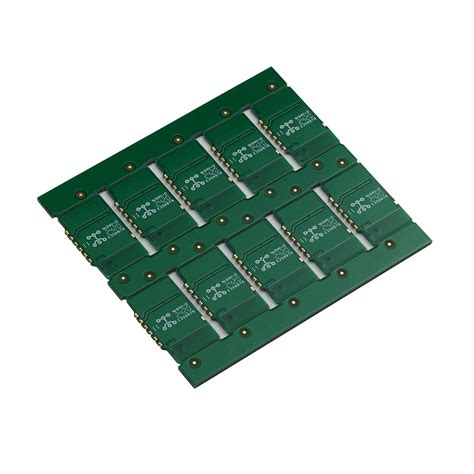
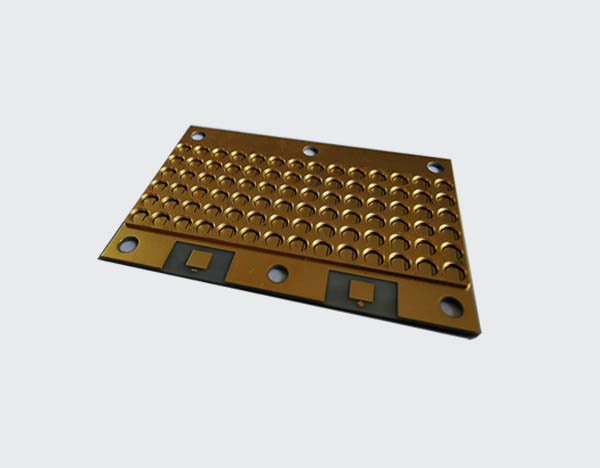
2.1 Basic Via Structure
A typical PCB via consists of several key components:
- Barrel: The conductive cylinder that forms the electrical connection between layers
- Pad: The annular ring connecting the barrel to traces on each layer
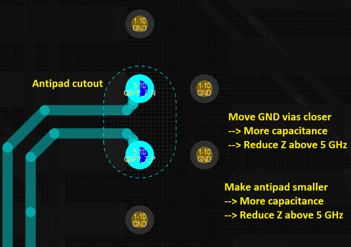
- Antipad: The clearance hole in adjacent layers to prevent unwanted connections
- Capture pad: The connection point on inner layers
2.2 Frequency-Dependent Behavior
At low frequencies, vias act as nearly ideal conductors. However, as frequency increases:
- The skin effect causes current to concentrate on the via’s outer surface
- Discontinuities in impedance create reflections
- Parasitic effects become significant
3. Parasitic Effects in High-Frequency Vias
3.1 Equivalent Circuit Model
A via can be modeled as a combination of:
- Inductance (L): Primarily from the via barrel (typically 0.1-1 nH)
- Capacitance (C): Between the via barrel and surrounding planes
- Resistance (R): Due to conductor losses and skin effect
- Conductance (G): Through the dielectric material
The impedance of a via can be calculated using:
Z = √( (R + jωL) / (G + jωC) )
3.2 Key Parasitic Elements
3.2.1 Via Inductance
The primary parasitic effect at high frequencies is inductance, given by:
L ≈ μ₀h/(2π) [ln(4h/d) + 1]
Where:
- μ₀ = permeability of free space (4π × 10⁻⁷ H/m)
- h = via length (height)
- d = via diameter
This inductance creates impedance discontinuities and slows signal edges.
3.2.2 Stub Effects
In multilayer boards, unused via portions (“stubs”) act as transmission line stubs that can resonate at certain frequencies, causing significant signal degradation.
3.2.3 Capacitive Effects
The capacitance between the via barrel and adjacent planes forms a low-pass filter that attenuates high-frequency components:
C ≈ (ε₀ε_rπd²)/(4h)
Where:
- ε₀ = permittivity of free space (8.854 × 10⁻¹² F/m)
- ε_r = dielectric constant of PCB material
- d = via pad diameter
- h = spacing between planes
3.2.4 Return Path Discontinuities
Vias can interrupt reference planes, forcing return currents to find alternative paths that may increase loop inductance and radiation.
4. Signal Integrity Impacts
4.1 Impedance Discontinuities
The combination of parasitic inductance and capacitance creates impedance mismatches that cause:
- Signal reflections (up to 20% of signal amplitude in some cases)
- Ringing on signal edges
- Increased jitter in digital systems
4.2 Attenuation and Loss Mechanisms
High-frequency signals experience:
- Conductor losses (skin effect and surface roughness)
- Dielectric losses in the substrate material
- Radiation losses from discontinuities
4.3 Crosstalk
Closely spaced vias can couple energy through:
- Electric field coupling (capacitive crosstalk)
- Magnetic field coupling (inductive crosstalk)
4.4 Resonance Effects
Stub portions of vias can create quarter-wave resonances that:
- Introduce deep notches in frequency response
- Cause significant signal degradation at resonant frequencies
5. Design Considerations for High-Frequency Vias
5.1 Via Geometry Optimization
- Diameter: Smaller diameters reduce capacitance but increase inductance
- Aspect ratio: Height/diameter ratio affects impedance and manufacturability
- Pad size: Minimize pad diameters to reduce capacitance
- Antipad size: Optimize clearance to balance capacitance and manufacturability
5.2 Via Transition Design
- Use controlled impedance via transitions matching the trace impedance
- Implement via fencing for critical signals
- Consider differential via pairing for differential signals
5.3 Stub Mitigation Techniques
- Back-drilling: Removal of unused via portions
- Buried vias: Only connect required layers
- Microvias: Laser-drilled vias connecting adjacent layers
- Via-in-pad: For high-density designs
5.4 Return Path Management
- Provide adjacent ground vias for signal transitions
- Ensure continuous reference planes near signal vias
- Use stitching vias to maintain low-impedance return paths
5.5 Material Considerations
- Low-loss dielectric materials (e.g., Rogers, Megtron)
- Smooth copper surfaces to reduce skin effect losses
- Consistent dielectric constant across frequency range
6. Advanced Via Technologies
6.1 Blind and Buried Vias
- Reduce stub effects by only connecting necessary layers
- Enable higher density interconnects
6.2 Microvias
- Smaller diameter (<100μm) vias with reduced parasitics
- Typically laser-drilled for precision
6.3 Via Fill Materials
- Conductive fills (copper, silver) to reduce impedance
- Non-conductive fills for planarization
6.4 Tapered Vias
- Gradual impedance transitions to minimize reflections
7. Simulation and Measurement Techniques
7.1 Modeling Approaches
- 3D electromagnetic field solvers (HFSS, CST)
- Transmission line models
- S-parameter analysis
7.2 Measurement Methods
- Time domain reflectometry (TDR)
- Vector network analyzer (VNA) measurements
- Eye diagram analysis for digital systems
8. Case Studies and Practical Examples
8.1 High-Speed Digital Applications
- DDR memory interfaces
- PCIe Gen 4/5 implementations
- 100G+ Ethernet systems
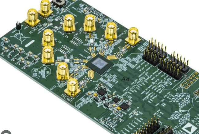
8.2 RF and Microwave Systems
- Millimeter-wave circuits (24-77 GHz)
- Antenna feed networks
- Filter implementations
9. Future Trends and Challenges
- Increasing frequencies (THz applications)
- Heterogeneous integration
- Advanced materials (low-loss, low-Dk)
- AI-assisted via optimization
10. Conclusion
PCB vias present significant challenges for high-frequency signal transmission, introducing parasitic effects that degrade signal integrity through impedance discontinuities, resonance, and loss mechanisms. However, through careful design incorporating optimized geometries, stub mitigation techniques, proper return path management, and advanced via technologies, these effects can be minimized. As signal frequencies continue to increase, the importance of via design will grow correspondingly, requiring designers to pay close attention to these critical interconnect elements. Future developments in materials, manufacturing processes, and design tools will provide additional capabilities to meet the challenges of next-generation high-frequency systems.