The Importance of PCB Copper Thickness in Electronic Design
Introduction to PCB Copper Thickness
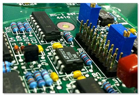
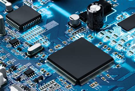
Printed Circuit Board (PCB) copper thickness is a critical parameter that significantly impacts the performance, reliability, and manufacturability of electronic devices. As the conductive medium that forms the pathways for electrical signals and power distribution, copper plays a fundamental role in PCB functionality. The thickness of this copper layer affects numerous aspects of board performance, from current carrying capacity to thermal management and signal integrity.
In modern electronics, where devices continue to shrink in size while increasing in complexity and power requirements, understanding and properly specifying copper thickness has become more important than ever. This article will explore the various aspects of PCB copper thickness, including measurement standards, design considerations, manufacturing implications, and performance characteristics.
Understanding Copper Weight and Thickness Measurements
Copper Weight: oz/ft²
PCB copper thickness is traditionally specified in ounces per square foot (oz/ft²), a measurement that dates back to the early days of printed circuit board manufacturing. This unit refers to the weight of copper that would cover one square foot of area if spread evenly. The most common copper weights used in PCBs include:
- 0.5 oz/ft² (17.5 μm)
- 1 oz/ft² (35 μm)
- 2 oz/ft² (70 μm)
- 3 oz/ft² (105 μm)
- 4 oz/ft² (140 μm)
Metric Equivalents
While the oz/ft² measurement remains standard in the industry, many designers and manufacturers also work with metric measurements in micrometers (μm) or millimeters (mm). The conversion between these units is straightforward:
1 oz/ft² = 35 μm (approximately)
1 μm = 0.0285 oz/ft²
Standard vs. Heavy Copper
PCBs are typically categorized based on their copper thickness:
- Standard PCBs: Generally use 0.5 oz/ft² to 2 oz/ft² copper
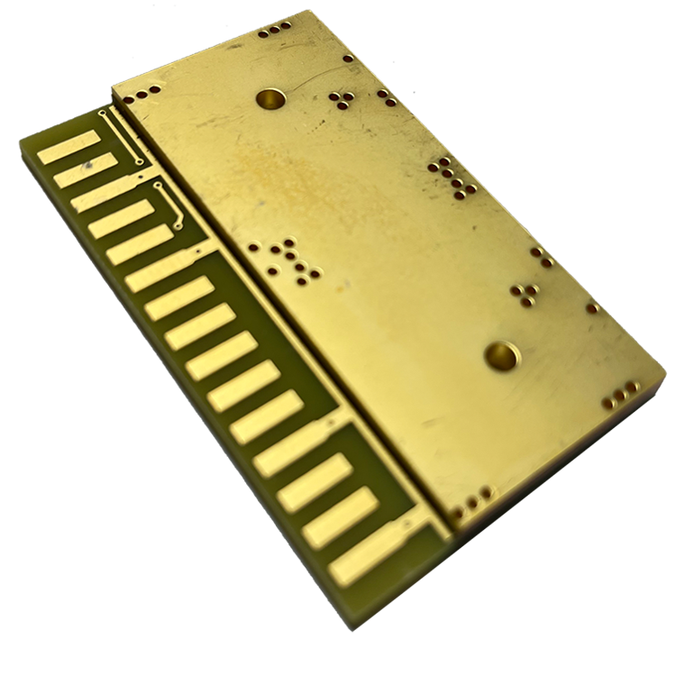
- Heavy Copper PCBs: Feature 3 oz/ft² or more, sometimes up to 20 oz/ft² for specialized applications
- Extreme Copper: A newer category exceeding 20 oz/ft² for very high-power applications
Factors Influencing Copper Thickness Selection
Current Carrying Capacity
One of the primary considerations when selecting copper thickness is the board’s current carrying requirements. Thicker copper can handle higher currents without excessive heating, as described by the IPC-2152 standard for determining current capacity in PCB conductors.
The relationship between copper thickness and current capacity isn’t linear—doubling the copper thickness doesn’t exactly double the current capacity due to thermal considerations and the skin effect at higher frequencies.
Thermal Management
Copper thickness significantly impacts a PCB’s thermal performance in several ways:
- Heat Distribution: Thicker copper layers help spread heat more evenly across the board
- Thermal Resistance: Reduced thermal resistance between components and heat sinks
- Power Dissipation: Ability to handle higher power levels without excessive temperature rise
For high-power applications, designers often use thicker copper or incorporate thermal relief patterns to manage heat effectively.
Signal Integrity Considerations
At high frequencies, copper thickness interacts with several signal integrity factors:
- Skin Effect: At high frequencies, current flows primarily near the conductor surface. The skin depth (δ) is given by:
δ = √(ρ/(πfμ))
where ρ is resistivity, f is frequency, and μ is permeability - Impedance Control: Copper thickness affects trace impedance calculations, particularly for microstrip and stripline configurations
- Insertion Loss: Thicker copper can reduce conductor losses, especially important for high-speed digital and RF applications
Manufacturing Constraints
Copper thickness impacts several manufacturing processes:
- Etching Tolerance: Thicker copper requires more aggressive etching, affecting minimum feature sizes
- Plating Uniformity: Achieving even copper distribution becomes more challenging with thicker layers
- Layer Registration: Thicker copper can affect alignment during multilayer lamination
Copper Thickness in Different PCB Layers
Outer Layers vs. Inner Layers
PCB fabrication typically involves different copper thicknesses for outer and inner layers:
- Outer Layers: Often start with 0.5 oz/ft² to 1 oz/ft² base copper, then are plated up to 1-2 oz/ft² during the plating process
- Inner Layers: Typically use 0.5 oz/ft² to 2 oz/ft² copper, with no additional plating
Multilayer Board Considerations
In multilayer boards, copper thickness selection must account for:
- Dielectric Requirements: Thicker copper affects the required dielectric spacing
- Via Reliability: Plated through-hole vias must accommodate different copper thicknesses
- Z-axis Expansion: Differential expansion rates between copper and dielectric materials
Manufacturing Processes and Copper Thickness
Copper Foil Production
PCB copper starts as foil produced through two primary methods:
- Electrodeposited (ED) Copper: The most common type, created through an electrochemical process
- Offers good adhesion
- Has a shiny side (drum side) and matte side
- Typical thickness range: 1/8 oz/ft² to 14 oz/ft²
- Rolled Annealed Copper: Created through physical rolling processes
- Smoother surface finish
- Better high-frequency performance
- Typically more expensive
PCB Fabrication Steps Affecting Copper Thickness
Several manufacturing steps influence final copper thickness:
- Initial Laminate Selection: Choosing the starting copper weight
- Pattern Plating: Adding copper to traces and pads during imaging
- Panel Plating: Uniform copper deposition across the entire panel
- Final Finishing: Processes like HASL or ENIG may add minimal thickness
Special Considerations for High-Power and High-Frequency Applications
Power Electronics
For power conversion and distribution applications, thick copper PCBs offer:
- Reduced Voltage Drop: Lower resistance paths for high currents
- Improved Thermal Performance: Better heat spreading and dissipation
- Increased Mechanical Strength: Thicker copper adds structural integrity
RF and Microwave Design
High-frequency designs require careful copper thickness consideration:
- Skin Depth Effects: At microwave frequencies, current flows in a thin surface layer
- Surface Roughness: Impacts insertion loss and phase characteristics
- Plating Quality: Voids or inconsistencies can degrade high-frequency performance
Testing and Verification of Copper Thickness
Common Measurement Methods
- Cross-Sectional Analysis: The most accurate but destructive method
- X-ray Fluorescence (XRF): Non-destructive measurement of copper weight
- Microwave Resonance: For non-contact thickness measurement
- Weight Difference Method: Measuring before and after copper removal
Industry Standards
Several standards govern copper thickness measurement and requirements:
- IPC-4562: Covers copper foil for printed circuit applications
- IPC-6012: Qualification and performance specification for rigid PCBs
- IPC-6018: For high-frequency (microwave) boards
Future Trends in PCB Copper Technology
Advanced Materials
- Reverse Treat Foils: Specialized copper foils for improved high-frequency performance
- Low-Profile Copper: Ultra-smooth surfaces for millimeter-wave applications
- Composite Copper Materials: Combining different materials for optimal performance
Manufacturing Innovations
- Additive Processes: Semi-additive and fully additive processes for precise copper deposition
- 3D Printed Electronics: New approaches to copper deposition in complex geometries
- Embedded Components: Integration of passive components within copper layers
Conclusion
PCB copper thickness remains a fundamental design parameter that balances electrical, thermal, mechanical, and manufacturing requirements. As electronic devices continue to evolve, pushing the boundaries of power density, signal speed, and miniaturization, the importance of proper copper thickness selection only grows.
Designers must consider the complex interplay between current requirements, signal integrity, thermal management, and manufacturability when specifying copper weights. With the emergence of new materials and manufacturing techniques, the options for copper implementation in PCBs continue to expand, offering engineers more tools to meet the demanding requirements of modern electronics.
Understanding the principles and practical implications of PCB copper thickness enables better design decisions, resulting in more reliable, higher-performance electronic products across all industries, from consumer electronics to aerospace applications.