The Importance of PCB Trace Width in PCB Design
Introduction
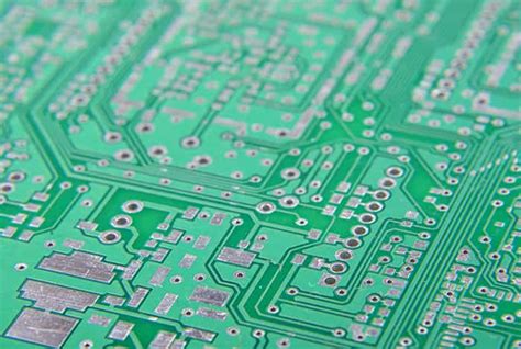
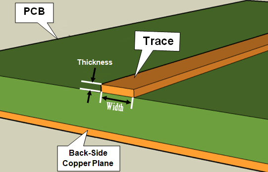
Printed Circuit Board (PCB) design is a complex engineering discipline that requires careful consideration of numerous factors to ensure optimal performance, reliability, and manufacturability. Among these critical factors, trace width stands out as one of the most fundamental yet often underestimated aspects of PCB design. PCB trace width—the physical width of the copper conductors that form electrical connections between components—plays a pivotal role in determining the board’s electrical characteristics, thermal management, signal integrity, and overall functionality.
This article will explore the multifaceted importance of trace width in PCB design, examining its impact on current carrying capacity, signal integrity, thermal management, impedance control, manufacturability, and cost considerations. By understanding these relationships, PCB designers can make informed decisions that balance performance requirements with practical constraints.
Current Carrying Capacity and Trace Width
One of the primary considerations when determining trace width is its current carrying capacity. The relationship between trace width and current capacity is governed by several physical principles and practical considerations:
Ohm’s Law and Resistance
The resistance of a trace is inversely proportional to its cross-sectional area (width × thickness). Narrower traces have higher resistance, which leads to greater voltage drop and power dissipation (I²R losses) when carrying current. This becomes particularly important in power distribution networks where even small voltage drops can affect circuit performance.
IPC Standards
The IPC-2152 standard provides guidelines for determining the current carrying capacity of PCB traces based on width, thickness, and allowable temperature rise. These standards account for:
- Internal vs. external traces (traces on outer layers can dissipate heat more easily)
- Copper weight (typically 0.5 oz/ft² to 2 oz/ft²)
- Ambient temperature and maximum allowable temperature rise
Practical Implications
Designers must calculate the appropriate trace width to:
- Prevent excessive heating that could damage the PCB or components
- Minimize voltage drops in power distribution networks
- Ensure reliable operation under maximum load conditions
For example, a typical 1 oz/ft² copper trace on an outer layer needs to be approximately 0.36mm (14 mil) wide to safely carry 1A of current with a 10°C temperature rise. Doubling the current requires approximately quadrupling the cross-sectional area.
Signal Integrity Considerations
Trace width significantly impacts signal integrity, especially in high-speed digital and high-frequency analog circuits:
Characteristic Impedance
In high-speed designs, traces act as transmission lines, and their width (along with other parameters) determines the characteristic impedance. Common impedance values (50Ω, 75Ω, 100Ω) must be maintained for proper signal transmission and to prevent reflections. The impedance depends on:
- Trace width
- Dielectric thickness (distance to reference plane)
- Dielectric constant of the PCB material
- Copper thickness
Signal Attenuation
Narrower traces have higher resistance, leading to greater attenuation of high-frequency signals. This becomes critical in:
- RF circuits
- High-speed digital interfaces (DDR, PCIe, USB)
- Long trace runs
Crosstalk
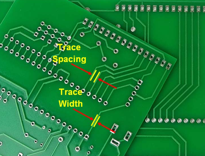
Proper trace width selection helps minimize crosstalk between adjacent signals:
- Wider spacing between traces reduces crosstalk but consumes more board space
- Controlled impedance designs often require specific width/spacing ratios
- Differential pairs require careful width and spacing control to maintain impedance

Thermal Management
Trace width plays a crucial role in the thermal performance of a PCB:
Heat Dissipation
Copper traces act as heat sinks for components:
- Wider traces can dissipate more heat from components
- Thermal relief connections must balance heat transfer with soldering requirements
Current Density and Heating
Excessive current density in narrow traces causes localized heating:
- Can lead to thermal stress and premature failure
- May cause solder joint degradation over time
- Can affect nearby temperature-sensitive components
Thermal Expansion
Different trace widths expand at different rates when heated:
- Wide power planes may cause board warping if not balanced
- Must consider in designs with large temperature variations
Manufacturability and Reliability
Trace width affects both the manufacturing process and the long-term reliability of the PCB:
Fabrication Limits
PCB manufacturers have minimum trace width capabilities:
- Standard PCBs typically support 6 mil (0.15mm) traces
- Advanced processes can achieve 3 mil (0.075mm) or less
- Minimum width affects cost and yield
Etching Considerations
The etching process has practical limitations:
- Very narrow traces may be under-etched or over-etched
- Aspect ratio (height to width) affects consistency
- Copper thickness must be considered with width
Reliability Factors
Proper trace width selection enhances reliability:
- Wider traces are more tolerant of manufacturing variations
- Reduce susceptibility to opens from minor etching defects
- Better withstand mechanical stress and vibration
High-Current Applications
Special considerations apply to high-current PCB designs:
Power Distribution
Wide traces or copper pours are used for:
- Power rails
- Ground planes
- High-current paths
Multiple Layers
Current can be distributed across multiple layers:
- Via stitching connects traces on different layers
- Must account for via resistance in current calculations
Alternative Approaches
When space constraints prevent wide traces:
- Use thicker copper (2 oz/ft² or more)
- Expose traces and add solder to increase cross-section
- Implement bus bars or external conductors
High-Frequency Considerations
At radio frequencies, additional factors come into play:
Skin Effect
At high frequencies, current flows primarily near the surface of conductors:
- Effective resistance increases with frequency
- Surface roughness becomes a factor
- May require special plating or treatment
Microstrip and Stripline
Different trace configurations have different width requirements:
- Microstrip (surface traces over a plane)
- Stripline (traces between two planes)
- Coplanar waveguide
Cost Implications
Trace width decisions impact PCB cost:
Material Usage
Wider traces use more copper but:
- May allow fewer layers in some designs
- Can reduce need for additional thermal management
Manufacturing Complexity
Tighter tolerances increase cost:
- Very narrow traces require more precise processes
- Impedance-controlled designs need tighter process control
Yield Considerations
Designs pushing fabrication limits may have lower yields:
- Affects overall product cost
- Impacts reliability and repair costs
Design Tools and Calculation Methods
Modern PCB design incorporates sophisticated tools for trace width optimization:
CAD Tools
PCB design software includes features for:
- Automated width selection based on design rules
- Real-time design rule checking (DRC)
- Impedance calculators
Simulation Capabilities
Advanced tools offer:
- Signal integrity simulation
- Thermal analysis
- Power distribution network analysis
Calculation Methods
Engineers use various methods to determine appropriate widths:
- IPC-2152 formulas and charts
- Online trace width calculators
- Empirical data from previous designs
Practical Design Guidelines
Based on the above considerations, here are some practical guidelines:
General Recommendations
- Always calculate required trace widths for power paths
- Use manufacturer’s capabilities as design constraints
- Consider both electrical and thermal requirements
Specific Scenarios
- Digital signals: Typically 8-12 mil for general routing
- Power traces: Calculate based on current requirements
- High-speed signals: Determine by impedance requirements
- RF signals: May require specialized width calculations
Best Practices
- Document trace width decisions in design specifications
- Include margin in width calculations for reliability
- Review manufacturing capabilities early in design process
Conclusion
PCB trace width is far more than just a dimensional parameter—it’s a critical design variable that affects nearly every aspect of board performance and reliability. From basic current carrying capacity to sophisticated high-speed signal integrity concerns, trace width decisions reverberate throughout the entire PCB design.
Successful PCB designers must understand the multifaceted relationships between trace width and electrical performance, thermal management, manufacturability, and cost. By applying this knowledge systematically—using appropriate calculations, design tools, and industry standards—engineers can optimize their designs for performance, reliability, and cost-effectiveness.
As PCB technology continues to evolve with higher densities, faster signals, and more demanding applications, the importance of proper trace width selection only grows. Mastering this fundamental aspect of PCB design remains essential for creating successful electronic products in an increasingly competitive and technologically sophisticated marketplace.