The Key Factors Determining the Quality of PCB Terminal Products
Introduction
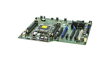
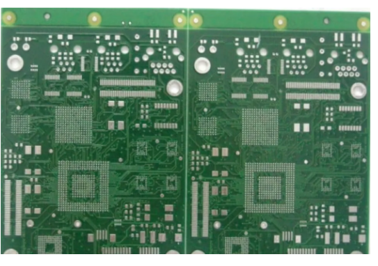
Printed Circuit Board (PCB) terminal products serve as critical components in virtually all modern electronic devices, from smartphones to industrial machinery. The quality of these PCB terminals directly impacts the performance, reliability, and longevity of the entire electronic system. As technology advances and devices become more complex, understanding what determines PCB terminal quality becomes increasingly important for manufacturers, engineers, and quality assurance professionals.
This article examines the key factors that determine the quality of PCB terminal products, covering material selection, design considerations, manufacturing processes, testing protocols, and environmental considerations. By analyzing these critical elements, we can better understand how to produce high-quality PCB terminals that meet the demanding requirements of today’s electronic applications.
1. Material Selection: The Foundation of Quality
The quality of PCB terminal products begins with the selection of appropriate materials, which form the foundation for all subsequent manufacturing processes and final product performance.
1.1 Base Material Composition
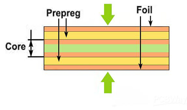
The base material of the PCB, typically a composite of woven fiberglass and epoxy resin (FR-4), significantly affects the terminal’s performance. High-quality base materials should offer:
- Excellent dielectric properties
- Thermal stability across operating temperatures
- Mechanical strength to withstand assembly processes
- Consistent thickness and flatness
For high-frequency applications, specialized materials like Rogers or Teflon-based substrates may be required to maintain signal integrity.
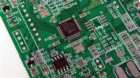
1.2 Copper Foil Quality
The copper foil used for conductive layers must meet strict requirements:
- Proper thickness (typically 0.5 oz to 2 oz per square foot)
- High purity (99.9% or better)
- Uniform grain structure
- Appropriate surface roughness for good adhesion
1.3 Surface Finishes
The choice of surface finish for terminals affects solderability, contact resistance, and durability:
- HASL (Hot Air Solder Leveling): Cost-effective but with limited flatness
- ENIG (Electroless Nickel Immersion Gold): Excellent for fine-pitch components
- Immersion Silver: Good solderability with moderate cost
- OSP (Organic Solderability Preservative): Economical but with limited shelf life
- Hard Gold: For high-wear contact areas
1.4 Solder Mask and Silkscreen
Quality solder mask materials provide:
- Proper insulation between conductors
- Resistance to environmental factors
- Good adhesion to the substrate
- Accurate registration with circuit patterns
2. Design Considerations: Engineering for Quality
Proper design is crucial for ensuring PCB terminal quality and encompasses multiple technical aspects.
2.1 Terminal Geometry and Layout
Well-designed terminals should feature:
- Appropriate pad sizes for reliable solder joints
- Proper spacing to prevent bridging or short circuits
- Consideration of current-carrying capacity
- Alignment with component leads or connectors
2.2 Thermal Management
Effective thermal design prevents overheating and ensures reliability:
- Proper copper distribution for heat dissipation
- Thermal relief connections for soldered terminals
- Consideration of thermal expansion coefficients
2.3 Signal Integrity
For high-speed applications, terminal design must maintain signal quality:
- Controlled impedance where needed
- Proper grounding schemes
- Minimization of stub lengths
- Careful routing to reduce crosstalk
2.4 Mechanical Considerations
Terminals must withstand physical stresses:
- Adequate anchor points for connectors
- Strain relief for flexible connections
- Robustness against insertion/removal forces
- Compatibility with mating components
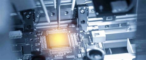
3. Manufacturing Processes: Precision Execution
Even with excellent materials and design, manufacturing processes ultimately determine the realized quality of PCB terminals.
3.1 Photolithography and Etching
Precise pattern transfer is essential:
- Accurate alignment of photomasks
- Proper exposure and development of photoresist
- Controlled etching to maintain trace dimensions
- Consistent copper thickness across the panel
3.2 Drilling and Hole Preparation
For through-hole terminals:
- Precise drill positioning and diameter control
- Clean hole walls free of debris or resin smear
- Proper hole-to-pad ratio
- Effective desmearing and cleaning processes
3.3 Plating Processes
High-quality plating ensures reliable terminals:
- Uniform copper deposition in through-holes
- Proper nickel and gold thickness for ENIG finishes
- Good adhesion between layers
- Absence of voids or nodules
3.4 Solder Mask Application
Quality solder mask application requires:
- Proper viscosity and thickness
- Accurate registration with circuit patterns
- Complete curing without under- or over-exposure
- Freedom from pinholes or bubbles
3.5 Surface Finish Application
Consistent surface finishes demand:
- Proper cleaning and preparation
- Controlled chemical baths
- Accurate thickness monitoring
- Thorough rinsing to prevent contamination
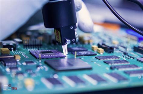
4. Quality Control and Testing: Verifying Performance
Rigorous testing protocols ensure that PCB terminals meet specifications and perform reliably in their intended applications.
4.1 Electrical Testing
Essential electrical tests include:
- Continuity testing to verify all connections
- Isolation testing to ensure proper insulation
- Impedance testing for controlled-impedance terminals
- Current-carrying capacity verification
4.2 Visual Inspection
Automated Optical Inspection (AOI) and manual checks examine:
- Surface defects like scratches or stains
- Solder mask integrity
- Plating quality
- Dimensional accuracy
4.3 Microsection Analysis
Cross-sectional analysis verifies:
- Plating thickness and uniformity
- Hole wall quality
- Layer-to-layer registration
- Material integrity
4.4 Environmental Testing
Reliability testing may include:
- Thermal cycling
- Humidity exposure
- Mechanical stress tests
- Chemical resistance evaluations
4.5 Solderability Testing
Terminal solderability is verified through:
- Wetting balance tests
- Dip-and-look methods
- Solder float tests
5. Environmental and Operational Considerations
The intended operating environment significantly influences the quality requirements for PCB terminals.
5.1 Temperature Requirements
Terminals must perform across expected temperature ranges:
- High-temperature stability for power applications
- Low-temperature performance for cold environments
- Resistance to thermal cycling effects
5.2 Humidity and Chemical Exposure
For harsh environments, terminals may need:
- Enhanced corrosion resistance
- Specialized conformal coatings
- Protection against chemical exposure
- Fungus resistance for certain applications
5.3 Mechanical Stress Conditions
Depending on application, terminals must withstand:
- Vibration and shock
- Flexing or bending stresses
- Repeated insertion/removal cycles
- Abrasion or wear
5.4 Long-term Reliability
Quality terminals maintain performance over time:
- Resistance to tin whisker growth
- Minimal contact resistance drift
- Stable insulation properties
- Durability against environmental aging
Conclusion
The quality of PCB terminal products is determined by a complex interplay of factors spanning material science, engineering design, precision manufacturing, and rigorous testing. No single element can ensure quality alone; rather, it is the careful consideration and execution of all these aspects that produces reliable, high-performance PCB terminals.
From the selection of base materials with appropriate electrical and mechanical properties to the implementation of controlled manufacturing processes and comprehensive quality assurance protocols, each step in the production chain contributes to the final product quality. Furthermore, the growing complexity of electronic devices and the increasing demands for miniaturization, high-speed performance, and reliability in harsh environments continue to raise the bar for PCB terminal quality.
Manufacturers who invest in understanding and controlling these key factors will produce PCB terminal products that meet today’s demanding applications while being prepared for the challenges of tomorrow’s electronic designs. Ultimately, the quality of PCB terminals reflects not just technical specifications, but the commitment to excellence throughout the entire design and production process.