The Major Design Challenges in PCB Development
Printed Circuit Boards (PCBs) are the backbone of modern electronics, serving as the foundation for everything from consumer gadgets to industrial machinery. However, designing a reliable and efficient PCB is a complex task that involves overcoming several critical challenges. This article explores the most significant PCB design challenges engineers face today, including signal integrity, thermal management, electromagnetic interference (EMI), power distribution, high-speed design, and manufacturability.
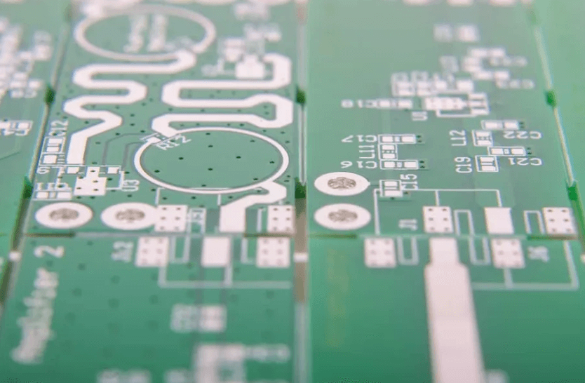
1. Signal Integrity Issues
Signal integrity (SI) refers to the quality of electrical signals as they travel through PCB traces. Poor signal integrity can lead to data corruption, timing errors, and system failures. Key challenges include:
A. Crosstalk
When signals from one trace interfere with adjacent traces due to electromagnetic coupling, it results in crosstalk. High-speed signals and densely packed PCBs are particularly susceptible.
Solutions:
- Increase trace spacing.
- Use ground planes to isolate signals.
- Implement differential signaling for noise immunity.
B. Impedance Mismatch
High-frequency signals require controlled impedance to prevent reflections. Mismatched impedance can distort signals, especially in RF and high-speed digital circuits.
Solutions:
- Use impedance calculators to design trace widths and dielectric materials.
- Match trace impedance with source and load components.
C. Signal Attenuation
High-frequency signals lose energy as they travel through PCB traces, leading to attenuation.
Solutions:
- Use low-loss dielectric materials (e.g., Rogers or Teflon-based substrates).
- Minimize trace length and avoid sharp bends.
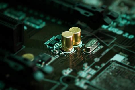
2. Thermal Management
Excessive heat can degrade component performance and reduce PCB lifespan. Managing heat dissipation is crucial for reliability.
A. Hotspots and Thermal Stress
High-power components (e.g., CPUs, FPGAs, power regulators) generate significant heat, creating hotspots.
Solutions:
- Use thermal vias to conduct heat to inner layers or heatsinks.
- Incorporate copper pours for better heat distribution.
B. Thermal Expansion Mismatch
Different materials expand at different rates when heated, leading to mechanical stress and potential solder joint failure.
Solutions:
- Select materials with similar coefficients of thermal expansion (CTE).
- Use flexible PCBs or strain relief techniques in high-temperature environments.
3. Electromagnetic Interference (EMI) and Compatibility (EMC)
EMI disrupts circuit performance, while EMC ensures the PCB does not interfere with other devices.
A. Radiated and Conducted EMI
High-speed signals and switching power supplies generate electromagnetic noise.
Solutions:
- Implement proper grounding techniques (star grounding, ground planes).
- Use shielding cans or ferrite beads for noise suppression.
B. PCB Layout and EMI
Poor routing can turn traces into unintended antennas.
Solutions:
- Keep high-speed traces short and away from sensitive analog circuits.
- Use ground planes beneath high-frequency traces to reduce radiation.
4. Power Distribution Network (PDN) Design
Ensuring stable power delivery is critical, especially in high-current applications.
A. Voltage Drop and IR Drop
Long power traces introduce resistance, leading to voltage drops.
Solutions:
- Use wider traces or power planes for low-resistance paths.
- Place decoupling capacitors near power-hungry ICs.
B. Power Supply Noise
Switching regulators introduce ripple, affecting sensitive analog circuits.
Solutions:
- Implement LC filters to smooth power delivery.
- Use low-ESR capacitors for better noise suppression.
5. High-Speed PCB Design Challenges
Modern electronics demand faster data rates, introducing new complexities.
A. Signal Skew and Timing Issues
In high-speed parallel buses (e.g., DDR memory), mismatched trace lengths cause timing skew.
Solutions:
- Use length-matching techniques (serpentining).
- Employ equalization and pre-emphasis in high-speed serial links.
B. Transmission Line Effects
At high frequencies, traces behave like transmission lines, requiring careful termination.
Solutions:
- Use proper termination resistors (series or parallel).
- Avoid stubs and discontinuities in high-speed paths.

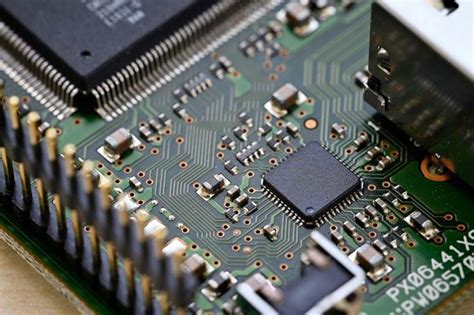
6. Manufacturability and Assembly Issues
A well-designed PCB must also be manufacturable at scale.
A. Design for Manufacturing (DFM) Errors
Incorrect pad sizes, insufficient clearances, or unrealistic tolerances lead to assembly defects.
Solutions:
- Follow manufacturer design rules (e.g., minimum trace width, drill sizes).
- Use automated DFM checks in PCB design software.
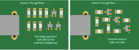
B. Component Placement and Soldering Challenges
Dense layouts make soldering difficult, increasing the risk of shorts or cold joints.
Solutions:
- Maintain adequate spacing between components.
- Use solder mask and paste layers effectively.
C. Mixed-Signal Layout Challenges
Combining analog and digital circuits requires careful isolation to prevent noise coupling.
Solutions:
- Separate analog and digital ground planes with a single-point connection.
- Route analog traces away from high-speed digital signals.
Conclusion
PCB design is a multidisciplinary challenge that requires balancing electrical performance, thermal management, EMI control, and manufacturability. Engineers must stay updated with evolving technologies such as high-speed digital interfaces, flexible PCBs, and advanced materials. By addressing these key challenges through best practices and simulation tools, designers can create robust, high-performance PCBs that meet the demands of modern electronics.
As PCB technology continues to advance, new challenges will emerge, but a strong foundation in these fundamental principles will remain essential for successful designs.