The Meaning and Design Challenges of PCB Copper
Introduction
Printed Circuit Boards (PCBs) are the backbone of modern electronics, providing mechanical support and electrical connections for electronic components. One of the most critical materials in PCB manufacturing is copper, which serves as the conductive pathway for electrical signals. The proper use of copper in PCB design significantly impacts the board’s performance, reliability, and manufacturability.
This article explores the meaning of PCB copper, its role in circuit design, and the key challenges engineers face when designing PCBs with copper traces, planes, and pads.
The Role of Copper in PCBs
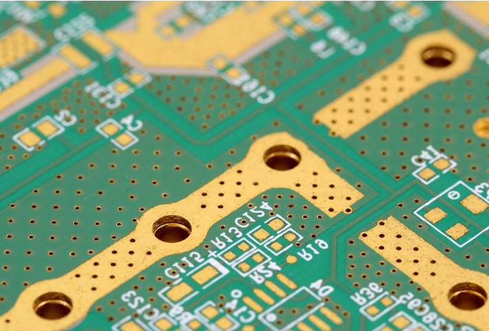
Copper is the primary conductive material used in PCBs due to its excellent electrical conductivity, thermal properties, and cost-effectiveness. It forms the conductive pathways (traces), pads, and planes that connect different components on the board.
1. Copper Traces
- These are thin lines of copper that carry electrical signals between components.
- Width and thickness determine current-carrying capacity and impedance.
2. Copper Planes (Power and Ground Planes)
- Large copper areas provide low-impedance power distribution and heat dissipation.
- Reduce electromagnetic interference (EMI) by acting as shielding layers.
3. Copper Pads and Vias
- Pads provide connection points for component leads.
- Vias are plated copper holes that connect different PCB layers.
The amount of copper used in a PCB is measured in ounces per square foot (oz/ft²), with common thicknesses being 0.5 oz, 1 oz, and 2 oz.
Key Design Challenges with PCB Copper
While copper is essential for PCB functionality, its use introduces several design and manufacturing challenges. Below are the most critical difficulties engineers must address.
1. Copper Thickness and Current Carrying Capacity
- Challenge: Thin traces may overheat or fail under high current.
- Solution: Use trace width calculators based on IPC-2152 standards to determine appropriate thickness.
2. Signal Integrity and Impedance Control
- Challenge: High-speed signals require controlled impedance traces.
- Solution: Precise trace width, dielectric material selection, and reference plane management.
3. Thermal Management
- Challenge: Excessive current can cause copper to heat up, leading to thermal stress.
- Solution: Use thermal relief pads, copper pours, and heat sinks.
4. Electromagnetic Interference (EMI) and Crosstalk
- Challenge: High-frequency signals can induce noise in adjacent traces.
- Solution: Proper grounding, spacing, and shielding techniques.
5. Manufacturing Tolerances and Etching Issues
- Challenge: Over-etching can lead to thinner traces, while under-etching causes shorts.
- Solution: Follow Design for Manufacturing (DFM) guidelines and work closely with PCB fabricators.
6. Copper Balancing for Multilayer PCBs
- Challenge: Uneven copper distribution can cause warping during lamination.
- Solution: Symmetrical copper distribution and proper stack-up design.
7. High-Frequency and RF Considerations
- Challenge: Skin effect increases resistance at high frequencies.
- Solution: Use thicker copper or specialized surface treatments.
8. Corrosion and Oxidation Prevention
- Challenge: Exposed copper can oxidize, leading to poor solderability.
- Solution: Apply surface finishes like ENIG (Electroless Nickel Immersion Gold) or HASL (Hot Air Solder Leveling).
Conclusion
Copper is a fundamental material in PCB design, enabling electrical connectivity and thermal management. However, its use introduces challenges related to current handling, signal integrity, thermal dissipation, EMI, and manufacturability. Engineers must carefully consider copper thickness, trace geometry, and layout strategies to ensure reliable PCB performance.
By understanding these challenges and applying best practices in PCB design, manufacturers can produce high-quality boards that meet the demands of modern electronics.