The Necessity of PCB Anti-Static Design: Protecting Electronics in an Electrified World
Introduction
In today’s increasingly digital and connected world, printed circuit boards (PCBs) serve as the fundamental building blocks of nearly all electronic devices. From smartphones and computers to medical equipment and automotive systems, PCBs form the intricate nervous systems that enable modern technology to function. However, these sophisticated electronic components face a silent but potentially devastating threat: electrostatic discharge (ESD). This article explores the critical necessity of incorporating anti-static design principles into PCB development, examining the risks of ESD, industry standards, design strategies, and real-world implications of proper electrostatic protection.
Understanding Electrostatic Discharge (ESD) and Its Threats to PCBs
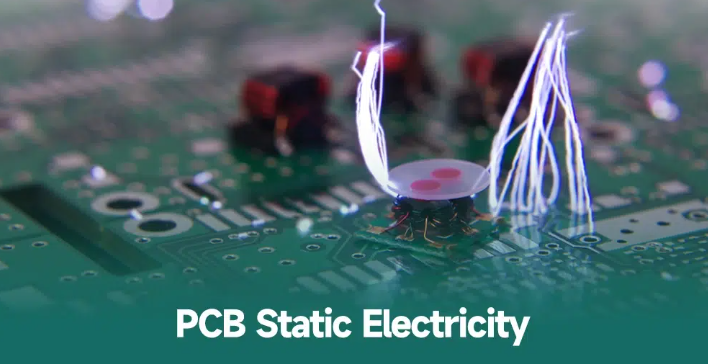
Electrostatic discharge refers to the sudden flow of electricity between two electrically charged objects caused by contact, an electrical short, or dielectric breakdown. In the context of PCBs, ESD typically occurs when static electricity accumulated on a person’s body, tools, or other objects discharges onto the board’s components or traces.
The dangers of ESD to PCBs manifest in several ways:
- Component Damage: Modern electronic components, particularly semiconductors and integrated circuits, have become increasingly sensitive to electrostatic discharge due to shrinking geometries and thinner oxide layers. A static shock that might have been harmless to components from a decade ago can now destroy contemporary chips.
- Latent Defects: Not all ESD damage is immediately apparent. Some components may suffer “walking wounded” damage—partial degradation that doesn’t cause immediate failure but significantly reduces the component’s lifespan and reliability.
- Signal Integrity Issues: ESD can induce electromagnetic interference (EMI) that disrupts signal transmission on PCB traces, leading to data corruption or system malfunctions.
- Manufacturing Yield Reduction: In production environments, ESD events can dramatically decrease manufacturing yields, increasing costs and delaying product deliveries.
The human body can easily generate static charges of several thousand volts through ordinary activities like walking across a carpet (1,500-35,000V) or handling plastic bags (1,200-20,000V). Meanwhile, many modern electronic components can be damaged by discharges as low as 100 volts, with some sensitive devices vulnerable to just 10 volts.
Industry Standards and Requirements for ESD Protection
Recognizing the severe consequences of ESD, various international standards organizations have established guidelines and requirements for ESD protection in electronic design:
- ANSI/ESD S20.20: This American national standard provides requirements for establishing an ESD control program to protect electrical and electronic parts, assemblies, and equipment.
- IEC 61340-5-1: The International Electrotechnical Commission’s standard for the protection of electronic devices from electrostatic phenomena.
- JEDEC Standards: The Joint Electron Device Engineering Council provides test methods for ESD sensitivity classification (JESD22-A114 for Human Body Model, JESD22-A115 for Machine Model, etc.).
- MIL-STD-883: The U.S. military standard that includes test methods for ESD sensitivity classification.
These standards typically classify components based on their ESD sensitivity and specify handling requirements accordingly. For example, components might be categorized as:
- Class 0: <250 volts
- Class 1A: 250-500 volts
- Class 1B: 500-1,000 volts
- Class 1C: 1,000-2,000 volts
- Class 2: 2,000-4,000 volts
- Class 3A: 4,000-8,000 volts
- Class 3B: ≥8,000 volts
Designing PCBs to meet these standards isn’t merely about compliance—it’s about ensuring product reliability, reducing warranty claims, and protecting brand reputation.
Essential PCB Anti-Static Design Strategies
Effective ESD protection in PCB design requires a multi-layered approach incorporating various strategies:
1. Proper Grounding Techniques
- Implement a solid ground plane to provide low-impedance paths for ESD currents
- Use star grounding for sensitive analog circuits
- Ensure proper connection between digital and analog grounds when necessary
2. Component Selection and Placement
- Choose components with built-in ESD protection when available
- Place sensitive components away from board edges and connectors
- Group components by their ESD sensitivity levels
3. Trace Routing Considerations
- Avoid long, uninterrupted traces that can act as antennas for ESD energy
- Maintain adequate trace spacing to prevent flashover
- Use curved rather than right-angle traces to minimize charge accumulation
4. ESD Protection Devices
- Transient voltage suppressor (TVS) diodes: Fast-acting devices that clamp ESD voltages
- Varistors: Voltage-dependent resistors that provide overvoltage protection
- Spark gaps: Small intentional gaps that allow controlled discharge
- Polymer ESD suppressors: Newer devices offering low capacitance and fast response
5. Board Layout Techniques
- Implement guard rings around sensitive components
- Use proper clearance and creepage distances
- Include discharge paths for connectors and user-interface elements
6. Layer Stackup Design
- Incorporate ground planes adjacent to signal layers
- Use power plane segmentation strategically
- Consider embedded capacitance for high-speed designs

The Cost-Benefit Analysis of PCB Anti-Static Design
While implementing robust ESD protection adds some complexity and cost to PCB design, the long-term benefits far outweigh these initial investments:
- Manufacturing Benefits:
- Higher production yields (reduced ESD-related failures during assembly)
- Lower testing and rework costs
- Improved consistency in product quality
- Product Reliability Advantages:
- Longer mean time between failures (MTBF)
- Reduced field failures and warranty claims
- Better performance in harsh environments
- Brand Protection:
- Enhanced reputation for quality and reliability
- Reduced risk of product recalls
- Improved customer satisfaction and loyalty
- Regulatory Compliance:
- Easier certification processes
- Access to markets with strict ESD requirements
- Reduced liability risks
The incremental cost of adding ESD protection elements like TVS diodes or optimizing board layout is typically minimal compared to the potential costs of ESD-related failures, which can include not just component replacement but also product recalls, brand damage, and lost customer trust.
Real-World Consequences of Inadequate ESD Protection
Numerous industry examples demonstrate the severe consequences of neglecting proper ESD protection in PCB design:
- Automotive Electronics Failures: In one documented case, a vehicle’s electronic control unit (ECU) experienced intermittent failures traced to ESD damage during assembly. The resulting recall affected over 100,000 vehicles, costing the manufacturer millions in repairs and reputational harm.
- Medical Device Malfunctions: A hospital reported unexplained resets in patient monitoring equipment, later attributed to ESD events when medical staff touched the devices. The manufacturer had to redesign the PCBs with better ESD protection and retrofit existing units.
- Consumer Electronics Returns: A smartphone manufacturer faced an unusually high return rate for devices with “mysterious” failures. Investigation revealed that many failures stemmed from ESD damage during normal handling, requiring a PCB redesign to incorporate more robust ESD protection.
- Industrial Control System Downtime: A factory experienced random shutdowns of its automated production line, eventually traced to ESD-induced failures in control system PCBs. The downtime cost exceeded $500,000 before the issue was resolved through proper ESD protection measures.
These cases underscore that ESD-related failures often manifest as intermittent, hard-to-diagnose problems that can persist throughout a product’s lifecycle if not addressed at the design stage.
Emerging Trends and Future Considerations in PCB ESD Protection
As electronic technology continues to evolve, so do the challenges and solutions for ESD protection:
- Miniaturization Challenges: With components shrinking to nanometer scales and operating voltages decreasing, devices become more ESD-sensitive even as board space for protection components diminishes.
- High-Speed Design Implications: Faster signal speeds (e.g., 5G, PCIe Gen 5) require ESD protection devices with lower capacitance, driving innovation in protection technologies.
- Flexible and Stretchable Electronics: The rise of flexible PCBs introduces new ESD protection challenges as traditional rigid-board solutions may not apply.
- Advanced Materials: Researchers are developing new materials with inherent ESD protection properties, such as conductive polymers and nanocomposites.
- System-Level ESD Simulation: Improved simulation tools allow designers to model ESD events and their impact on complete systems before prototyping.
- IoT and Edge Device Considerations: The proliferation of connected devices in diverse environments increases exposure to ESD risks, requiring robust yet cost-effective solutions.
Conclusion
In the intricate world of PCB design, electrostatic discharge protection is not an optional enhancement but a fundamental requirement for reliable, durable electronic products. The increasing sensitivity of modern electronic components, coupled with the ever-present nature of static electricity in our environment, makes comprehensive ESD protection essential at every stage—from initial design through manufacturing to end-use.
Effective PCB anti-static design requires a holistic approach combining proper grounding strategies, careful component selection and placement, strategic use of protection devices, and adherence to industry standards. While implementing these measures requires additional design effort and potentially some incremental cost, the alternative—ESD-related failures in the field—invariably proves far more costly in terms of repairs, recalls, reputation damage, and lost customer trust.
As electronic systems continue to permeate every aspect of modern life, from mission-critical medical equipment to ubiquitous consumer devices, the importance of robust PCB anti-static design will only grow. By prioritizing ESD protection from the earliest design stages, engineers can create products that not only survive in our electrified world but thrive throughout their intended service life. In this context, PCB anti-static design isn’t merely about preventing failures—it’s about enabling the reliable operation of the technologies that power our digital age.


