The Open-Source PCB Revolution: Exploring the Potential of Solder Mask-Free Designs
Introduction
In the world of printed circuit board (PCB) design and manufacturing, a quiet revolution is taking place as makers, hobbyists, and even some professional engineers begin exploring the possibilities of open-source PCBs without solder mask layers. This movement challenges conventional PCB manufacturing wisdom and opens up new possibilities for accessibility, customization, and innovation in electronics development.
Solder mask—that familiar green (or sometimes red, blue, or black) coating covering most commercial PCBs—has long been considered an essential part of circuit board fabrication. However, the growing open-source hardware movement is now questioning this assumption, demonstrating how eliminating this layer can make PCB production more accessible while maintaining functionality for many applications.
Understanding Solder Mask and Its Traditional Role
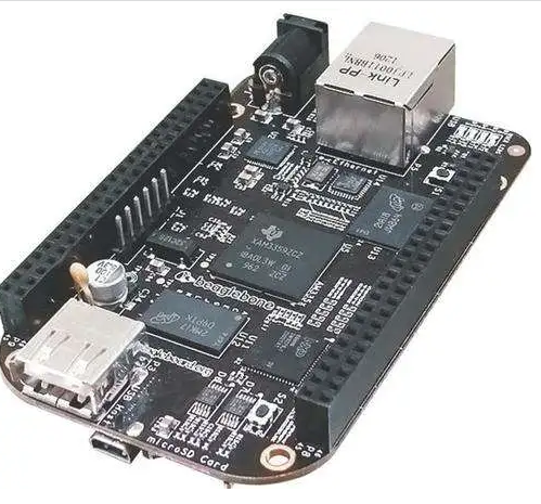
Before examining the implications of removing solder mask, it’s important to understand what this layer does in conventional PCB design:
Primary Functions of Solder Mask:
- Prevents solder bridges between closely spaced pads during assembly
- Protects copper traces from oxidation and environmental damage
- Provides electrical insulation between conductors
- Improves aesthetics and provides color coding
- Gives structural support to surface mount components
Manufacturing Considerations:
- Adds complexity to the fabrication process
- Requires precise alignment (especially for fine-pitch components)
- Introduces additional material costs
- Needs curing/processing steps
- Limits DIY fabrication options
The solder mask application process typically involves screen printing, spray coating, or dry film application followed by UV exposure and development. This requires specialized equipment not generally available to hobbyists or small-scale makers.
The Case for Solder Mask-Free Open-Source PCBs
The movement toward open-source, solder mask-free PCB designs presents several compelling advantages:
1. Increased Accessibility and DIY Potential
Without the need for solder mask application, PCB fabrication becomes significantly more accessible to:
- Makers and hobbyists working in home labs
- Educators teaching electronics in schools with limited budgets
- Developers in resource-constrained environments
- Researchers needing rapid, low-cost prototyping
2. Simplified Manufacturing Process
Eliminating solder mask removes:
- Alignment challenges for double-sided boards
- Curing/development steps
- Specialized application equipment requirements
- Mask-related defects (misregistration, incomplete curing)
3. Cost Reduction
Removing solder mask can reduce PCB costs by:
- Eliminating mask material expenses
- Reducing equipment costs for small-scale producers
- Minimizing processing steps
- Allowing use of lower-cost fabrication methods
4. Enhanced Modifiability
Open copper surfaces allow for:
- Easier circuit modifications and repairs
- Simpler addition of hand-soldered components
- More accessible probing and debugging
- Flexible post-production changes to traces
5. Environmental Considerations
Some solder mask formulations contain chemicals of environmental concern. Mask-free designs:
- Reduce chemical usage
- Simplify board recycling
- Eliminate mask disposal issues
Technical Considerations for Solder Mask-Free Designs
While the benefits are significant, designing effective PCBs without solder mask requires addressing several technical challenges:
1. Preventing Solder Bridges
Solutions include:
- Increased pad-to-pad spacing (wider pitch components)
- Strategic use of solder thieves (additional copper areas)
- Careful solder paste application
- Selective hand soldering
2. Trace Protection Alternatives
Options for protecting exposed copper:
- Conformal coatings (can be brushed or sprayed)
- Lacquers or clear nail polish
- Wax-based coatings
- Natural oxidation (for temporary prototypes)
3. Component Selection Guidelines
- Prefer larger pitch components (≥1.27mm recommended)
- Avoid ultra-fine pitch ICs (QFP, BGA packages)
- Consider through-hole components where possible
- Select larger SMT packages (0805, 1206 sizes)
4. Design Rule Adjustments
Recommended modifications:
- Increase clearance rules (≥0.5mm where possible)
- Widen traces where practical
- Use teardrops at pad-trace junctions
- Include solder relief gaps in ground planes
Successful Applications of Mask-Free Open PCBs
Several notable open-source hardware projects have successfully implemented solder mask-free designs:
1. Educational Platforms
- Arduino-style development boards for classroom use
- Basic logic and analog circuit trainers
- Introductory SMT soldering practice boards
2. Low-Consumer Electronics
- Simple sensor nodes and data loggers
- Basic audio amplifiers and filters
- LED drivers and lighting controllers
3. Prototyping Systems
- Breadboard-alternative development platforms
- Modular circuit building blocks
- Experimental analog computing systems
4. Specialized Research Tools
- Custom lab equipment interfaces
- One-off scientific instrumentation
- Reconfigurable test fixtures
Challenges and Limitations
While solder mask-free designs offer many advantages, they aren’t suitable for all applications:
Technical Limitations:
- Not suitable for high-density designs
- Challenging with fine-pitch components (<0.8mm)
- Reduced durability in harsh environments
- Higher risk of accidental shorts
Manufacturing Considerations:
- Manual assembly requires more skill
- Limited suitability for wave soldering
- Reduced compatibility with pick-and-place machines
- Shorter shelf life due to copper oxidation
Commercial Viability Issues:
- May not meet certain industry standards
- Limited appeal for mass-produced consumer goods
- Potential reliability concerns for critical applications
The Future of Open-Source Mask-Free PCBs
As the open-source hardware movement grows, we can expect several developments:
1. Improved Design Methodologies
- Specialized design rule sets for mask-free boards
- Development of hybrid approaches (partial masking)
- Better CAD tools supporting mask-free workflows
2. New Materials and Processes
- Advanced oxidation-resistant copper treatments
- Easier-to-apply protective coatings
- Improved solder paste formulations
3. Expanded Applications
- More complex educational platforms
- Greater adoption in scientific instrumentation
- Increased use in art and interactive installations
4. Community Development
- Shared repositories of mask-free designs
- Best practice documentation
- Specialized forums and knowledge bases
Conclusion
The movement toward open-source, solder mask-free PCB designs represents an important development in democratizing electronics manufacturing. By removing barriers to entry and simplifying fabrication processes, these approaches make circuit board production more accessible to makers, educators, and developers worldwide.
While not suitable for all applications, solder mask-free designs fill an important niche in the electronics ecosystem—particularly for education, prototyping, and low-volume specialized applications. As the methodology matures and more designers contribute to the open-source knowledge base, we can expect to see continued innovation in this space.
The success of mask-free open PCBs demonstrates that sometimes, removing complexity can be the most innovative approach of all. In an era where accessibility and sustainability are becoming increasingly important, these designs offer a compelling alternative to conventional PCB manufacturing paradigms.

