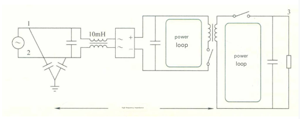
The PCBA assembly and welding process of FPC is different from that of rigid circuit boards.
5.Inspection, testing and board separation of FPC:
Since the carrier board absorbs heat in the furnace, especially the aluminum carrier board, the temperature is high when it comes out of the furnace, so it is best to add a forced cooling fan at the furnace outlet to help cool down quickly. At the same time, the operator needs to wear heat-insulating gloves to avoid being scalded by the high-temperature carrier board. When taking the soldered FPC from the carrier board, apply force evenly and do not use brute force to avoid tearing or creases on the FPC.
Put the removed FPC under a magnifying glass with a magnification of more than 5 times for visual inspection, focusing on problems such as residual glue on the surface, discoloration, tinning of gold fingers, tin beads, empty soldering of IC pins, and continuous soldering. Since the surface of the FPC cannot be very flat, the misjudgment rate of AOI is very high, so FPC is generally not suitable for AOI inspection, but with the help of special test fixtures, FPC can complete ICT and FCT tests.
Since FPC is mostly connected boards, it may be necessary to separate the boards before testing ICT and FCT. Although the separation operation can be completed using tools such as blades and scissors, the operation efficiency and quality are low, and the scrap rate is high. If it is a mass production of special-shaped FPC, it is recommended to make a special FPC stamping board splitting mold for stamping and splitting, which can greatly improve the work efficiency. At the same time, the edges of the punched FPC are neat and beautiful, and the internal stress generated during the punching and cutting is very low, which can effectively avoid solder joint tin cracking.
In the assembly and welding process of PCBA flexible electronics, the precise positioning and fixation of FPC are the key points. The key to good fixation is to make a suitable carrier board. The second is the pre-baking, printing, patch and reflow soldering of FPC. Obviously, the SMT process of FPC is much more difficult than that of PCB hard board, so it is necessary to accurately set the process parameters. At the same time, strict production process management is equally important. It is necessary to ensure that the operators strictly implement every regulation in the SOP. The line engineers and IPQC should strengthen inspections, promptly discover abnormal conditions of the production line, analyze the causes and take necessary measures to control the defective rate of the FPC SMT production line within dozens of PPM.
In the PCBA production process, it is necessary to rely on a lot of machines and equipment to assemble a board. Often the quality level of a factory’s machines and equipment directly determines the manufacturing capacity.
The basic equipment required for PCBA production includes solder paste printer, chip mounter, reflow soldering, AOI detector, component foot cutting machine, wave soldering, tin furnace, board washer, ICT test fixture, FCT test fixture, aging test rack, etc. The equipment equipped by PCBA processing plants of different sizes will be different.
6. PCBA production equipment
(1)Solder paste printer
Modern solder paste printers are generally composed of mechanisms such as plate loading, solder paste adding, stamping, and circuit board feeding. Its working principle is: first fix the circuit board to be printed on the printing positioning table, and then the left and right scrapers of the printer will print the solder paste or red glue through the steel mesh on the corresponding pads. For the PCB with uniform leakage, it will be input to the chip mounter through the transmission table for automatic chip mounting.
(2)Chip mounter
The chip mounter: also known as “mounting machine” or “surface mount system” (Surface Mount System). In the production line, it is configured after the solder paste printer. It is a device that accurately places surface mount components on the PCB pads by moving the mounting head. It is divided into manual and fully automatic.
(3)Reflow soldering
There is a heating circuit inside the reflow soldering, which heats the air or nitrogen to a high enough temperature and blows it to the circuit board with the components already attached, so that the solder on both sides of the components melts and bonds with the main board. The advantage of this process is that the temperature is easy to control, oxidation can be avoided during the welding process, and the manufacturing cost is easier to control.
(4)AOI detector
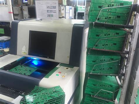
AOI (Automatic Optic Inspection) is the full name of automatic optical inspection, which is a device based on optical principles to detect common defects encountered in welding production. AOI is a new type of testing technology that has just emerged, but it has developed rapidly, and many manufacturers have launched AOI testing equipment. When automatically inspecting, the machine automatically scans the PCB through a camera, collects images, compares the tested solder joints with the qualified parameters in the database, and checks the defects on the PCB through image processing, and displays/marks the defects through a display or automatic mark for maintenance personnel to repair.
5.Component pin cutting machine
It is used to cut and deform the pin components.
6.Wave soldering
Wave soldering is to make the soldering surface of the plug-in board directly contact with high-temperature liquid tin to achieve the purpose of soldering. The high-temperature liquid tin maintains an inclined surface, and a special device makes the liquid tin form a wave-like phenomenon, so it is called “wave soldering”. Its main material is solder bar.
7.Tin furnace
Generally speaking, tin furnace refers to a soldering tool used in electronic soldering. It has good soldering consistency for discrete component circuit boards, convenient and fast operation, and high work efficiency. It is a good helper for your production and processing.
8.Board washing machine
It is used to clean PCBA boards and remove the residues on the boards after soldering.
9.ICT Test Fixture
ICT Test mainly uses the test probe to contact the test points on the PCB layout to detect the open circuit, short circuit, and welding of all parts of the PCBA
10.FCT Test Fixture
FCT (Functional Test) refers to a test method that provides a simulated operating environment (excitation and load) to the test target board (UUT: Unit Under Test) to make it work in various design states, thereby obtaining the parameters of each state to verify the function of the UUT. Simply put, it is to load the UUT with appropriate excitation and measure whether the output response meets the requirements.
11.Aging Test Stand
Aging test stands can test PCBA boards in batches, and test problematic PCBA boards by simulating user operations for a long time.
PCBA outsourcing refers to the PCBA processing manufacturer outsourcing the PCBA order to other powerful PCBA processing manufacturers. So, what are the general requirements for PCBA outsourcing?
- Bill of Materials
Components should be inserted or mounted strictly in accordance with the bill of materials, PCB silk screen printing and outsourcing processing requirements, when the material does not match the list, PCB silk screen, or contradicts the process requirements, or the requirements are unclear and cannot be operated, you should contact our company in time to confirm the correctness of the material and process requirements.
II. Anti-static requirements
- All components are treated as electrostatic sensitive devices.
- All personnel who come into contact with components and products must wear anti-static clothing, anti-static wristbands, and anti-static shoes.
- During the raw material entry and storage stage, electrostatic sensitive devices are all packaged in anti-static packaging.
- During the operation, use an anti-static work surface, and use anti-static containers to hold components and semi-finished products.
- The welding equipment is reliably grounded, and the electric soldering iron is anti-static. All must be tested before use.
- Anti-static boxes are used for storage and transportation of semi-finished PCB boards, and anti-static pearl cotton is used as isolation materials.
- Anti-static packaging bags are used for complete machines without shells.
III. Provisions on the insertion direction of component appearance identification
- Polar components are inserted according to polarity.
- When the components with screen printing on the side (such as high-voltage ceramic capacitors) are inserted vertically, the screen printing faces right; when inserted horizontally, the screen printing faces downward. When the components with screen printing on the top (excluding chip resistors) are inserted horizontally, the font direction is the same as the screen printing direction of the PCB board; when inserted vertically, the top of the font faces right.
- When the resistor is inserted horizontally, the error color ring faces right; when inserted horizontally, the error color ring faces downward; when the resistor is inserted vertically, the error color ring faces the board surface.
IV. Welding requirements
- The pin height of the inserted component on the welding surface is 1.5~2.0mm. The chip component should be flat against the board surface, the solder joint should be smooth without burrs and slightly arc-shaped, and the solder should exceed 2/3 of the height of the solder end, but should not exceed the height of the solder end. Less tin, spherical solder joints or solder-covered patches are all bad;
- Solder joint height: The height of solder climbing pins should not be less than 1mm for single-sided boards, and not less than 0.5mm for double-sided boards, and tin should be penetrated.
- Solder joint shape: Conical and covered with the entire pad.
- Solder joint surface: Smooth and bright, without black spots, flux and other debris, without spikes, pits, pores, exposed copper and other defects.
- Solder joint strength: Fully wetted with pads and pins, no false solder joints or false solder joints.
- Solder joint cross section: When cutting the component pins, try not to cut the solder part, and there should be no tin cracking on the contact surface between the pins and the solder. There are no spikes or barbs at the cross section.
- Needle seat welding: The needle seat requires the bottom board to be inserted, and the position is correct and the direction is correct. After the needle seat is welded, the bottom floating height does not exceed 0.5mm, and the seat body is skewed and does not exceed the silk screen frame. The rows of needle seats should also be kept neat, and no front-to-back misalignment or unevenness is allowed
V. Transportation
To prevent PCBA damage, the following packaging should be used during transportation:
- Container: anti-static turnover box.
- Isolation material: anti-static pearl cotton.
- Placement spacing: There is a distance of more than 10mm between PCB boards and between PCB boards and boxes.
- Placement height: There is a space of more than 50mm from the top of the turnover box to ensure that the turnover box does not press the power supply when stacking, especially the power supply with wires.
VI. Board washing requirements
The board surface should be clean, without tin beads, component pins, and stains. Especially at the solder joints on the plug-in surface, no dirt left by welding should be seen. When washing the board, the following devices should be protected: wires, connecting terminals, relays, switches, polyester capacitors and other easily corrosive devices, and relays are strictly prohibited from being cleaned with ultrasonic waves.
VII. All components are not allowed to exceed the edge of the PCB board after installation.
When the PCBA passes through the furnace, the pins of the plug-in components are washed by the tin flow, and some plug-in components will be tilted after passing through the furnace for soldering, causing the component body to exceed the silk screen frame. Therefore, the repair personnel behind the tin furnace are required to make appropriate corrections.