The precautions about the wiring of copper print pcb
Current density of wiring : Most electronic circuits are now made of copper-bonded insulating boards. The copper thickness of commonly used circuit boards is 35μm. The current density value of the wiring can be taken according to the empirical value of 1A/mm. The specific calculation can be referred to the textbook.
In order to ensure the mechanical strength of the wiring,
the line width should be greater than or equal to 0.3mm (other non-power circuit boards may have a smaller minimum line width). The copper thickness is 70μm. Circuit boards are also commonly used in switching power supplies, so the current density can be higher.
In addition, the commonly used circuit board design tool software generally has design specification items, such as line width, line spacing, dry plate via size and other parameters can be set. When designing circuit boards, the design software can automatically execute according to the specifications, which can save a lot of time, reduce some workload, and reduce the error rate.
Generally, double-sided boards can be used for circuits with relatively high reliability requirements or high wiring line density.
Its characteristics are moderate cost, high reliability, and can meet most applications.
Some products in the module power supply line also use multi-layer boards, which are mainly convenient for integrating power devices such as transformer inductors, optimizing wiring, and power tube heat dissipation. It has the advantages of good consistency of process and good heat dissipation of transformers, but its disadvantages are high cost and poor flexibility, and it is only suitable for industrial large-scale production.
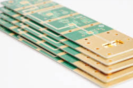
Single-sided board, almost all general switching power supplies in the market use single-sided circuit boards, which have the advantage of low cost, and some measures in design and production process can also ensure its performance.
Today, let’s talk about some experience in the design of single-sided printed circuit boards. Because single-sided boards have the characteristics of low cost and easy manufacturing, they are widely used in switching power supply circuits. Since they only have one side of copper bonding, the electrical connection and mechanical fixation of the device all rely on that layer of copper skin, and care must be taken when handling them.
In order to ensure good welding mechanical structure performance, the single-sided board pad should be slightly larger to ensure good bonding between the copper skin and the substrate, so as not to peel off or break off the copper skin when it is vibrated. Generally, the width of the welding ring should be greater than 0.3mm. The diameter of the pad hole should be slightly larger than the diameter of the device pin, but not too large, to ensure the shortest distance between the pin and the pad by solder connection. The size of the pad hole should not hinder normal inspection. The pad hole diameter is generally 0.1-0.2mm larger than the pin diameter. Multi-pin devices can also be larger to ensure smooth inspection.
Electrical connections should be as wide as possible. In principle, the width should be larger than the pad diameter.
In special cases, the line must be widened (commonly known as generating teardrops) when the connection line intersects with the pad to avoid the line and pad from breaking under certain conditions. The minimum line width should be greater than 0.5mm in principle.
Components on single-sided boards should be close to the circuit board.
For devices that require overhead heat dissipation, sleeves should be added to the pins between the device and the circuit board, which can play a dual role of supporting the device and increasing insulation. It is necessary to minimize or avoid the impact of external force on the connection between the pad and the pin to enhance the firmness of welding. For components with heavier weight on the circuit board, support connection points can be added to strengthen the connection strength between the circuit board, such as transformers and power device heat sinks.
The pins on the welding surface of a single-sided board can be left longer without affecting the spacing with the shell.
The advantage is that it can increase the strength of the welding part, increase the welding area, and detect cold welding immediately. When the pins are cut, the welding part is less stressed. In Taiwan and Japan, the process of bending the device pins on the welding surface to a 45-degree angle with the circuit board and then welding is often used. The reason is the same as above. Today, let’s talk about some matters in the design of double-sided boards. In some application environments with higher requirements or higher wiring density, double-sided printed boards are used, and their performance and various indicators are much better than single-sided boards.
Double-sided board pads have higher strength due to metallization treatment of holes.
The solder ring can be smaller than that of single-sided boards, and the pad hole diameter can be slightly larger than the pin diameter, because it is conducive to the solder solution to penetrate through the solder hole to the top pad during the soldering process to increase the soldering reliability. However, there is a disadvantage. If the hole is too large, some components may float up under the impact of jet tin during wave soldering, resulting in some defects.
For high current traces, the line width can be processed according to the previous post. If the width is not enough, it can generally be solved by tinning the trace to increase the thickness. There are many methods.
- Set the trace to the pad attribute, so that the trace will not be covered by the solder mask during the circuit board manufacturing, and will be tinned during hot air leveling.
- Place the pad at the wiring location and set the pad to the shape of the required trace. Be careful to set the pad hole to zero.
- Place the trace on the solder mask layer. This method is the most flexible, but not all circuit board manufacturers will understand your intentions. Textual instructions are required. Solder mask will not be applied to the part where the trace is placed on the solder mask layer.
Several methods of tinning the trace are as above.
It should be noted that if a very wide trace is tinned, a large amount of solder will be adhered after soldering, and the distribution will be very uneven, affecting the appearance. Generally, a thin strip of tin plating with a width of 1~1.5mm can be used, and the length can be determined according to the circuit. The interval of the tin plating part is 0.5~1mm. The double-sided circuit board provides a lot of options for layout and routing, which can make the wiring more reasonable. Regarding grounding, the power ground and the signal ground must be separated. The two grounds can be combined at the filter capacitor to avoid large pulse currents passing through the signal ground connection and causing unexpected unstable factors. The signal control loop should use a single point grounding method as much as possible. There is a trick to place the non-grounded wiring on the same wiring layer as much as possible, and finally lay the ground wire on another layer. The output line generally passes through the filter capacitor first, and then to the load. The input line must also pass through the capacitor first, and then to the transformer. The theoretical basis is to let the ripple current pass through the filter capacitor.
Voltage feedback sampling, in order to avoid the influence of large current passing through the wiring,
the sampling point of the feedback voltage must be placed at the end of the power supply output to improve the load effect index of the whole machine.
The wiring from one wiring layer to another is generally connected by vias,
and it is not suitable to be realized through the device pin pads, because this connection relationship may be destroyed when the device is inserted. In addition, there should be at least 2 vias for every 1A current passing through. The via diameter should be greater than 0.5mm in principle, and generally 0.8mm can ensure processing reliability.
Device heat dissipation, in some low-power power supplies, the circuit board routing can also have a heat dissipation function. Its characteristics are that the routing is as wide as possible to increase the heat dissipation area, and no solder resist is applied. If conditions permit, the vias can be evenly placed to enhance the thermal conductivity.