The process review is becoming more and more difficult. How can we cut the Gordian knot?
On-site process is the backbone of the product manufacturing process of PCBA factories. On-site process personnel must identify the difficulties of product manufacturing in advance, prevent and control various potential design defects, and ensure that the products are produced in the most economical way.
This is the core work of on-site process. As electronic products become thinner and smaller, component welding terminals and PCB pads are also getting smaller and smaller. On-site process review is becoming more and more important and more difficult.

What are the process difficulties of SMT?
Printing solder paste is the core of SMT. The quality of solder paste printing determines the quality of welding, so the steel mesh opening is the key.
The steel mesh opening design should be combined with PCB pads, solder mask, silk screen, device welding terminal characteristics, adjacent device distribution, adjacent exposed copper distribution, and pads in large copper foil areas.
Printing, patching, and welding of fine-pitch devices are relatively difficult and prone to problems, so the welding quality of fine-pitch devices determines the quality of products.
Fine-pitch devices should not only consider the stability of tin printing, but also consider the false welding caused by printing and patching after tinning, and slight deviation of patches. Eliminating the tiny printing gap of fine-pitch devices cannot be ignored. This is the core of the printing solder paste process (Teacher Jia Zhongzhong calls this the process in the SMT process, which shows its significant impact).
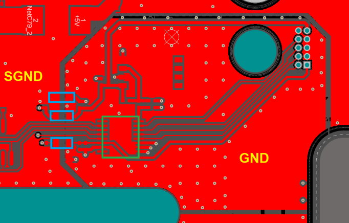
The close spacing between the SMD printed tin pad and the exposed through hole is prone to solder loss, resulting in false soldering and insufficient tin.
The necessary avoidance of holes, reduction of openings, and fine-tuning of opening positions can avoid problems.
The small spacing between SMD printed tin pads is prone to printing tinning and tinning after patching. The necessary reduction of openings and fine-tuning of opening positions can avoid problems.
SMD pads with small areas and close spacing will make it difficult to open the steel mesh. At this time, not only the opening area ratio and the safe spacing between openings should be considered, but also the tiny printing gap and the risk of solder overflow when the solder of the pad defined by the solder mask melts.
The tiny pads defined by the solder mask are prone to solder overflow and tinning.
Via holes on SMD printed tin pads are a bad design, especially for BTC devices. When welding via holes blocked with solder mask at the bottom of the pad, bubbles often get out of control; bare via holes will cause solder loss, resulting in false soldering and insufficient soldering, which leads to countless poor soldering, so necessary hole avoidance has to be done.
The following takes the common problem of printing tiny pads as an example to briefly describe its process difficulties, improvement methods, and efficient review methods.
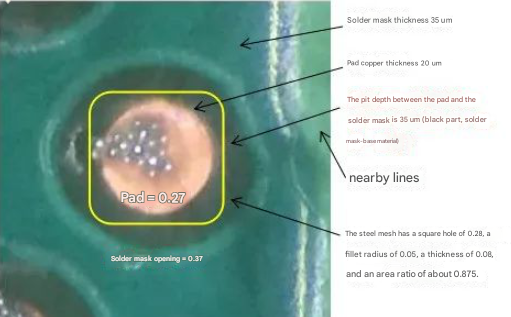
Process difficulties: tiny pads, difficult printing, potential tin leakage/insufficient tin problems
Root cause of the problem: There is a printing gap between the tiny pad and the steel mesh
Improvement method:
Pad design: Increase the pad diameter (0.27 changes to 0.31), reduce the area of the deep pit around the pad, so that the opening area originally on the deep pit becomes on the pad copper foil, and the gap between the opening area originally on the deep pit and the bottom of the steel mesh is reduced (verified OK).
Solder mask thickness: Reduce the PCB solder mask thickness to reduce the influence of the high solder mask layer on the circuit near the pad. It is recommended that the PCB solder mask thickness be less than 25um.
Use a new PH steel mesh to eliminate the printing gap to the maximum extent.
Note: In this case, the printing gap caused by solder mask is the cause of the problem. This type of problem is most easily overlooked. Eliminating the printing gap of tiny pads, especially eliminating the printing gap caused by PCB routing and solder mask, is the key to solving this type of problem.