The Purpose of PCB Exposure in the Printed Circuit Board Manufacturing Process
Introduction
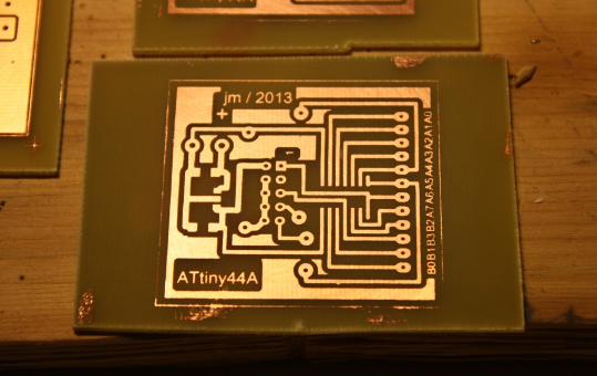
Printed Circuit Board (PCB) manufacturing is a complex, multi-step process that requires precision and attention to detail. One of the most critical stages in PCB fabrication is the exposure process, which plays a vital role in transferring the desired circuit pattern onto the board. Exposure is a photolithographic technique that ensures the accurate replication of circuit designs onto the copper-clad laminate before etching.
This article explores the purpose of PCB exposure, the underlying principles, the types of exposure methods used, and the factors that influence exposure quality. By understanding this process, manufacturers can optimize PCB production for better performance, reliability, and yield.
1. Understanding the PCB Exposure Process
Before delving into the purpose of exposure, it is essential to understand where it fits into the overall PCB fabrication process.
1.1 Key Steps Before Exposure
- Substrate Preparation – A copper-clad laminate is cleaned to remove contaminants.
- Photoresist Application – A light-sensitive chemical (photoresist) is applied to the copper surface.
- Pre-Baking – The board is heated to evaporate solvents and solidify the photoresist.
1.2 The Exposure Step
After applying the photoresist, the PCB is covered with a photomask (or film) containing the circuit pattern. The board is then exposed to ultraviolet (UV) light. The UV light hardens (for negative photoresist) or softens (for positive photoresist) the exposed areas, creating a latent image of the circuit.
1.3 Steps After Exposure
- Development – The unexposed photoresist is washed away, revealing the copper underneath.
- Etching – The exposed copper is removed, leaving only the desired circuit traces.
- Stripping – The remaining photoresist is removed, finalizing the conductive pattern.
2. The Primary Purpose of PCB Exposure
The exposure process serves several critical functions in PCB manufacturing:
2.1 Precise Pattern Transfer
The main purpose of exposure is to accurately transfer the circuit design from the photomask to the photoresist-coated PCB. The UV light modifies the photoresist’s chemical properties, allowing the subsequent development step to remove only the unwanted areas. This precision ensures that fine traces, pads, and vias are correctly formed.
2.2 Enabling High-Resolution Features
Modern PCBs require extremely fine traces (sometimes as small as 2 mils or 50 microns). Exposure allows for:
- High-density interconnects (HDI) – Essential for advanced electronics like smartphones and IoT devices.
- Controlled impedance traces – Critical for high-frequency and RF applications.
Without precise exposure, these tiny features would suffer from undercutting, bridging, or incomplete etching.
2.3 Ensuring Consistency Across Multiple Layers
Multi-layer PCBs require perfect alignment between layers. Exposure systems (especially laser direct imaging, LDI) ensure that each layer aligns precisely with drilled vias and internal connections. Misalignment can lead to short circuits or open connections.
2.4 Facitating Different Photoresist Types
- Negative Photoresist – Hardens when exposed to UV light; unexposed areas are removed during development.
- Positive Photoresist – Softens when exposed; the exposed areas are washed away.
The exposure process must be optimized based on the photoresist type to ensure proper chemical reactions.
2.5 Minimizing Defects
Proper exposure reduces common PCB defects such as:
- Underexposure – Leads to incomplete resist hardening, causing etching issues.
- Overexposure – Can cause line width variations or resist peeling.
- Misalignment – Results in non-functional boards due to layer mismatches.
3. Types of PCB Exposure Methods
Different exposure techniques are used depending on PCB complexity and production volume:
3.1 Contact Printing
- A photomask is placed in direct contact with the PCB.
- Pros: Simple, low-cost.
- Cons: Mask wear, potential scratches, lower resolution.
3.2 Proximity Printing
- The mask is held slightly above the PCB (~10-50 microns gap).
- Pros: Reduces mask damage.
- Cons: Slight resolution loss due to light diffraction.
3.3 Projection Printing
- Uses lenses to project the mask image onto the PCB.
- Pros: High resolution, no mask contact.
- Cons: Expensive, complex alignment.
3.4 Laser Direct Imaging (LDI)
- A laser directly “draws” the circuit pattern without a physical mask.
- Pros: Highest precision, ideal for HDI and flexible PCBs.
- Cons: Higher equipment cost.
4. Factors Affecting Exposure Quality
Several variables must be controlled to achieve optimal exposure:
4.1 UV Light Intensity & Wavelength
- Different photoresists react to specific UV wavelengths (typically 365nm or 405nm).
- Insufficient intensity causes underexposure; excessive intensity leads to overexposure.
4.2 Exposure Time
- Too short → Incomplete curing.
- Too long → Overexposure and feature distortion.
4.3 Photomask Quality
- Dust, scratches, or misalignment on the mask lead to defects.
4.4 Photoresist Thickness
- Thicker resist requires longer exposure times.
4.5 Environmental Conditions
- Humidity and temperature can affect photoresist performance.
5. Conclusion
The exposure process in PCB manufacturing is crucial for accurate pattern transfer, high-resolution feature definition, and multi-layer alignment. Whether using traditional UV exposure or advanced LDI, manufacturers must optimize exposure parameters to avoid defects and ensure reliability.
As PCB technology advances—with finer pitches, higher densities, and more complex designs—the exposure process will continue to evolve, incorporating innovations like AI-driven alignment systems and faster laser imaging techniques. Understanding the fundamentals of exposure helps engineers and manufacturers produce high-quality PCBs for today’s demanding electronic applications.
By mastering this critical step, the electronics industry can push the boundaries of miniaturization, performance, and functionality in next-generation devices.