The Relationship Between Capacitor Cracking/Shorting on PCBA and Design Factors
Abstract
Capacitor cracking and subsequent short-circuiting on printed circuit board assemblies (PCBAs) are common failure modes that can lead to catastrophic system failures. While manufacturing and handling processes often receive blame, design-related factors play a significant role in these failures. This paper explores the relationship between PCBA design and capacitor cracking/shorting, analyzing key design considerations such as mechanical stress, thermal management, layout optimization, and material selection. By understanding these factors, engineers can implement design strategies to mitigate capacitor failures and enhance product reliability.
1. Introduction
Capacitors are critical components in electronic circuits, providing functions such as filtering, decoupling, and energy storage. However, multilayer ceramic capacitors (MLCCs) and other types are prone to cracking under mechanical or thermal stress, leading to short circuits. While external factors like mechanical shock and soldering stress contribute to these failures, poor design choices significantly increase the risk. This paper examines how design decisions influence capacitor reliability and provides recommendations to prevent cracking and shorting.
2. Causes of Capacitor Cracking and Shorting
Before analyzing design-related factors, it is essential to understand the primary causes of capacitor failures:
- Mechanical Stress: Excessive bending or flexing of the PCB can induce cracks in brittle ceramic capacitors.
- Thermal Stress: Rapid temperature changes or mismatched coefficients of thermal expansion (CTE) between the capacitor and PCB can cause fractures.
- Soldering Stress: Improper reflow profiles or excessive mechanical force during assembly may damage capacitors.
- Electrical Overstress: Voltage spikes or exceeding rated voltage can lead to dielectric breakdown.
While these factors are often attributed to manufacturing or environmental conditions, design choices can either mitigate or exacerbate them.
3. Design Factors Contributing to Capacitor Cracking and Shorting
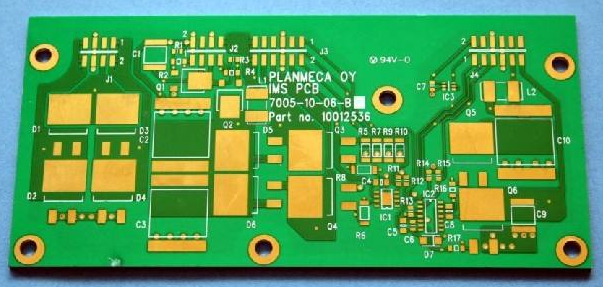
3.1 PCB Layout and Component Placement
The positioning of capacitors on the PCB significantly affects their susceptibility to stress:
- Proximity to Board Edges or Mounting Holes: Capacitors placed near high-stress areas (e.g., screw holes or board edges) are more likely to crack due to mechanical flexing.
- Orientation Relative to PCB Bend Lines: If the PCB undergoes flexing (e.g., in handheld devices), capacitors should be placed perpendicular to the bend axis to minimize stress.
- High-Density Areas: Overcrowding components can lead to uneven stress distribution during thermal cycling or mechanical shock.
Design Recommendation: Place capacitors away from high-stress zones and ensure proper spacing to allow for thermal expansion.
3.2 Thermal Management and CTE Mismatch
Thermal cycling is a major contributor to capacitor cracking due to CTE differences between the ceramic capacitor (6–8 ppm/°C) and the FR4 PCB (13–18 ppm/°C). Poor thermal design exacerbates this issue:
- Insufficient Thermal Relief: Lack of thermal vias or copper pours can lead to localized heating, increasing stress.
- Uneven Heating: Components near heat sources (e.g., power ICs) experience more thermal stress.
- Poor Reflow Profile Compliance: If the PCB design does not facilitate uniform heating during soldering, residual stresses may remain.
Design Recommendation: Use thermal vias, optimize copper distribution, and avoid placing capacitors near high-heat components.
3.3 Mechanical Reinforcement and Support Structures
The PCB’s mechanical rigidity influences capacitor reliability:
- Thin or Flexible PCBs: Thin boards (e.g., <1.6 mm) are more prone to bending, increasing capacitor stress.
- Lack of Stiffeners: Flexible PCBs without stiffeners may experience excessive flexing during assembly or operation.
- Improper Mounting: Inadequate support for large or heavy components can transfer stress to nearby capacitors.
Design Recommendation: Use thicker PCBs (≥1.6 mm) for rigid applications or add stiffeners in flexible designs.
3.4 Capacitor Selection and Sizing
Choosing the wrong capacitor type or size can increase cracking risk:
- Large-Form-Factor MLCCs: Larger capacitors (e.g., 1210 or larger) are more susceptible to mechanical stress than smaller ones (e.g., 0402 or 0603).
- High-Capacitance, Low-Voltage MLCCs: These have thinner dielectric layers, making them more prone to cracking under mechanical stress.
- Incorrect Voltage Rating: Using capacitors near their rated voltage increases the risk of dielectric breakdown under transient spikes.
Design Recommendation: Opt for smaller, higher-voltage-rated capacitors where possible, and distribute capacitance across multiple devices to reduce stress on individual components.
3.5 Solder Joint and Pad Design
Poor solder joint design can introduce stress concentrations:
- Overly Large or Small Pads: Mismatched pad sizes can lead to uneven solder distribution, increasing mechanical stress.
- Non-Compliant Solder Mask Definitions: Inadequate solder mask relief can cause stress points near terminations.
- Excessive Solder Paste: Too much solder can create mechanical strain during reflow.
Design Recommendation: Follow IPC-7351 pad design guidelines and ensure proper solder mask application.

4. Mitigation Strategies in PCBA Design
To minimize capacitor cracking and shorting, designers should adopt the following best practices:
- Optimize Component Placement:
- Keep capacitors away from high-stress areas (board edges, mounting holes).
- Orient capacitors to minimize bending stress.
- Improve Thermal Management:
- Use thermal vias and copper pours for even heat distribution.
- Avoid placing capacitors near high-power components.
- Enhance Mechanical Stability:
- Use thicker PCBs or stiffeners in flexible designs.
- Implement strain relief for connectors and heavy components.
- Select Robust Capacitors:
- Prefer smaller MLCCs where possible.
- Use higher-voltage-rated capacitors for margin.
- Follow Best Practices in Solder Joint Design:
- Adhere to IPC pad standards.
- Ensure proper solder mask application.
5. Conclusion
Capacitor cracking and shorting on PCBAs are not solely manufacturing or handling issues—design choices play a crucial role. By optimizing PCB layout, thermal management, mechanical support, and component selection, engineers can significantly reduce failure rates. Implementing these design strategies enhances product reliability, reduces field failures, and lowers warranty costs. Future work should focus on advanced simulation techniques (e.g., finite element analysis) to predict and mitigate stress-related failures early in the design phase.