The Relationship Between PCB Layer Count and Electromagnetic Compatibility (EMC)
Introduction
Printed Circuit Board (PCB) design has become increasingly complex in modern electronics, with one of the critical design considerations being electromagnetic compatibility (EMC). Among various factors affecting EMC, the number of layers in a PCB plays a significant role. This 2000-word article explores the intricate relationship between PCB layer count and EMC performance, examining how additional layers can both improve and potentially degrade a board’s electromagnetic characteristics.
Understanding PCB Layer Count and EMC Basics
PCB Layer Configurations
PCBs can range from simple single-layer designs to complex multilayer boards with dozens of layers. The most common configurations include:
- Single-layer (1-layer)
- Double-layer (2-layer)
- 4-layer
- 6-layer
- 8-layer and above
Each additional layer provides more routing options but also introduces new EMC considerations.
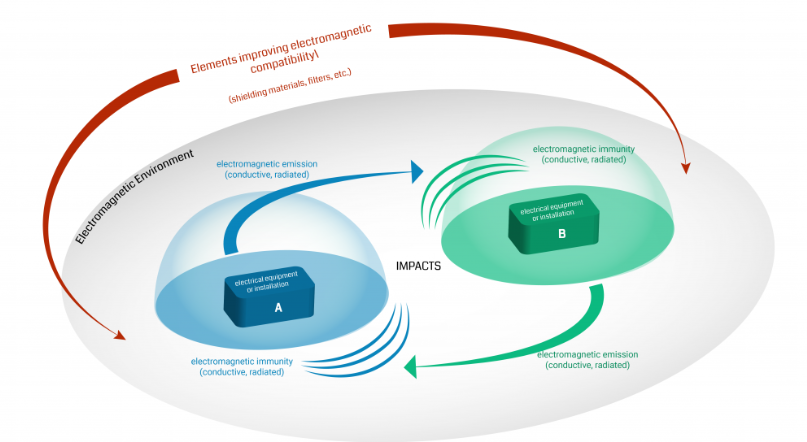
Electromagnetic Compatibility Fundamentals
EMC refers to a device’s ability to:
- Operate as intended in its electromagnetic environment (Immunity)
- Not produce electromagnetic disturbances that affect other devices (Emissions)
Key EMC aspects affected by PCB design include:
- Radiated emissions
- Conducted emissions
- Crosstalk
- Signal integrity
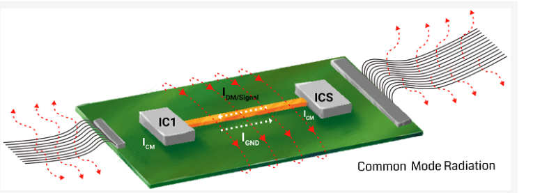
- Ground bounce
How Layer Count Affects EMC Performance
Ground and Power Planes
One of the most significant EMC benefits of multilayer PCBs is the ability to dedicate entire layers to ground and power planes:
4-layer boards typically use:
- Layer 1: Components and signals
- Layer 2: Ground plane
- Layer 3: Power plane
- Layer 4: Signals
This configuration provides:
- Improved return current paths
- Reduced ground impedance
- Better shielding between layers
- Controlled impedance for high-speed signals
6-layer boards often add:
- Additional ground planes
- Dedicated routing layers
- Better separation of analog and digital circuits
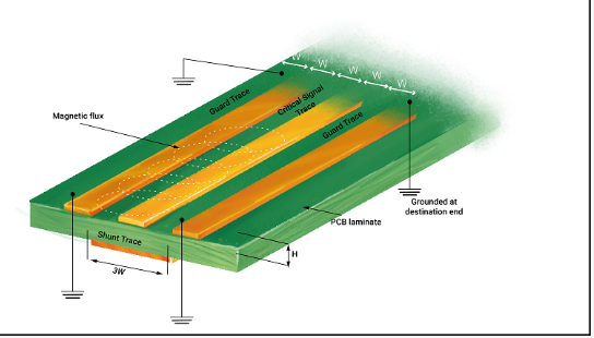
Signal Integrity Improvements
More layers allow for:
- Proper spacing between signal layers: Alternating signal layers with ground/power planes reduces crosstalk
- Controlled impedance: Essential for high-speed designs, easier to achieve with dedicated plane layers
- Shorter return paths: Minimizes current loop areas, reducing radiation
Current Return Path Management
A critical EMC factor is providing uninterrupted return paths for signals. Multilayer boards with continuous planes:
- Minimize loop areas (reducing antenna efficiency)
- Lower ground impedance (reducing ground bounce)
- Provide shielding between layers
Single and double-layer boards struggle with return path discontinuity, often leading to increased emissions.
Potential EMC Challenges with High Layer Counts
While additional layers generally improve EMC, certain challenges emerge:
Via Effects
More layers mean:
- Longer vias (acting as small antennas)
- More via stubs (causing signal reflections)
- Potential impedance discontinuities
Power Distribution Network (PDN) Complexity
High layer count boards require careful PDN design to:
- Maintain low impedance across all frequencies
- Prevent power plane resonances
- Manage decoupling capacitor placement
Interlayer Coupling
Despite shielding planes, very high layer counts can still experience:
- Capacitive coupling between non-adjacent layers
- Common impedance coupling through shared planes
- Simultaneous switching noise propagation
Layer Stackup Strategies for Optimal EMC
The arrangement of layers (stackup) is as important as the number of layers:
4-Layer Board EMC Optimization
Preferred stackup:
- Signal
- Ground (solid)
- Power (solid)
- Signal
Alternative (less optimal):
- Signal
- Signal
- Power
- Ground
6-Layer Board Configurations
Best EMC performance:
- Signal (microstrip)
- Ground
- Signal (stripline)
- Signal (stripline)
- Power
- Signal (microstrip)
8-Layer and Beyond
High-performance designs might use:
- Multiple ground planes
- Buried signal layers between planes
- Dedicated power plane pairs
- Symmetrical stackups to prevent warping
Practical Considerations for Layer Count Selection
Cost vs. EMC Performance
While more layers generally improve EMC, each additional layer increases cost. Designers must balance:
- EMC requirements
- Signal integrity needs
- Budget constraints
Signal Types and Speeds
- Low-speed designs (<25MHz) can often use 2-4 layers
- High-speed designs (>100MHz) typically require 6+ layers
- Mixed-signal designs benefit from separate ground planes
Industry Standards and Regulations
The required layer count depends on applicable EMC standards:
- FCC Part 15 (USA)
- CISPR (International)
- Military/aerospace standards (often requiring more layers)
Case Studies: Layer Count Impact on EMC
Case 1: Consumer IoT Device
Original 2-layer design:
- Failed radiated emissions at 450MHz
- Added ground fill improved but not enough
4-layer redesign:
- Dedicated ground plane
- Proper return paths
- Passed emissions with margin
Case 2: Automotive ECU
Initial 4-layer board:
- Marginal EMC performance
- Crosstalk issues between CAN and sensor lines
Upgraded to 6-layer:
- Additional ground plane
- Separated sensitive signals
- Met automotive EMC requirements
Advanced Techniques in High-Layer Count PCBs
Embedded Planes
Some high-layer count boards use embedded plane technology:
- Ultra-thin dielectric between power/ground
- Creates inherent decoupling capacitance
- Improves high-frequency PDN performance
Split Planes
Careful use of split planes can:
- Isolate noisy circuits
- Separate analog/digital grounds
- Must be implemented correctly to avoid creating slot antennas
Back Drilling
For very high layer counts (>12):
- Removes unused via stubs
- Reduces reflections
- Improves signal integrity at high frequencies
Future Trends: Layer Count and EMC
Emerging technologies are changing the relationship:
- Higher signal speeds: Requiring more layers for proper isolation
- Flex/rigid-flex PCBs: New challenges for maintaining EMC
- 3D packaging: Affecting traditional layer count approaches
- Advanced materials: Allowing fewer layers with better EMC performance
Conclusion
The relationship between PCB layer count and EMC is complex but crucial for modern electronic design. While additional layers generally improve EMC by providing better plane structures, controlled impedance, and reduced emissions, they must be implemented with careful stackup design and layout practices. The optimal layer count balances EMC requirements, signal integrity needs, and cost constraints. As electronics continue advancing in speed and complexity, understanding this relationship becomes ever more critical for successful product development that meets stringent EMC requirements.
Designers should:
- Start with EMC requirements when determining layer count
- Use appropriate stackup configurations
- Verify designs through simulation and testing
- Consider future scalability needs
By thoughtfully applying these principles, engineers can leverage PCB layer count as a powerful tool in achieving robust electromagnetic compatibility.