The Relationship Between PCB Trace Width, Current, and Temperature
Abstract
This paper explores the critical relationship between printed circuit board (PCB) trace width, current carrying capacity, and temperature rise in electronic circuit design. As electronic devices continue to shrink in size while demanding higher performance, understanding these interrelationships becomes increasingly important for reliable PCB design. The article examines the fundamental principles, presents relevant formulas and standards, discusses calculation methods, and provides practical design considerations for engineers. Through analysis of key parameters and their interactions, this paper offers guidance for optimizing PCB layouts to balance current requirements, thermal management, and space constraints.
1. Introduction
Printed Circuit Boards (PCBs) form the backbone of modern electronics, providing mechanical support and electrical connections between components. One of the most fundamental aspects of PCB design involves determining appropriate trace widths for various current-carrying conductors. The width of a PCB trace directly affects its current-carrying capacity and the resulting temperature rise during operation.
As electronic devices become more compact and power-dense, the proper sizing of PCB traces has grown increasingly critical. Traces that are too narrow for their current load can overheat, leading to reduced reliability or complete failure. Conversely, excessively wide traces waste valuable board space that could be used for other circuitry or component placement.
This paper examines the complex relationship between three key parameters:
- Trace width (measured in mils or millimeters)
- Current carrying capacity (measured in amperes)
- Temperature rise (measured in degrees Celsius above ambient)
Understanding these relationships allows designers to create PCBs that are both electrically sound and thermally stable.

2. Fundamental Principles
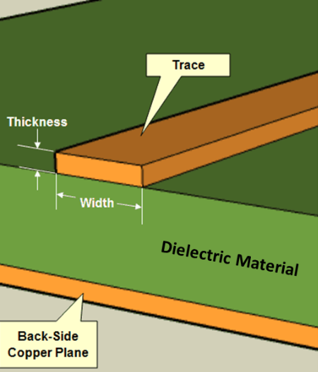
2.1 Electrical Resistance of PCB Traces
The current-carrying capacity of a PCB trace is fundamentally limited by its electrical resistance, which causes power dissipation in the form of heat when current flows. The resistance of a trace depends on three primary factors:
R = ρ × (L / (T × W))
Where:
- R = Resistance (Ω)
- ρ = Resistivity of copper (Ω·m)
- L = Length of the trace (m)
- T = Thickness of the trace (m)
- W = Width of the trace (m)
Standard PCB copper thickness is typically specified in ounces (oz), where 1 oz copper equals approximately 1.4 mils (0.035 mm) thickness.
2.2 Heat Generation and Dissipation
When current flows through a trace with resistance, power is dissipated as heat according to Joule’s law:
P = I² × R
Where:
- P = Power dissipated (W)
- I = Current (A)
- R = Resistance (Ω)
This heat generation must be balanced by heat dissipation through conduction, convection, and radiation to prevent excessive temperature rise.
2.3 Temperature Rise Considerations
The allowable temperature rise in a PCB depends on several factors:
- Material properties (especially the substrate’s glass transition temperature Tg)
- Operating environment
- Reliability requirements
- Safety standards
Common design practices typically limit temperature rises to 10-20°C above ambient for general applications, though specific cases may allow higher rises.
3. Standards and Calculation Methods
Several standards and methodologies exist for determining appropriate trace widths for given current loads and temperature rises.
3.1 IPC-2152 Standard
The IPC-2152 standard (“Standard for Determining Current-Carrying Capacity in Printed Board Design”) is the most widely accepted reference for PCB trace sizing. It provides comprehensive data on the relationship between trace width, current, and temperature rise based on extensive testing and empirical data.
Key aspects of IPC-2152 include:
- Consideration of both internal and external traces
- Accounting for copper thickness
- Incorporation of adjacent trace effects
- Provision for various dielectric materials
3.2 Simplified Calculation Methods
While the full IPC-2152 standard provides the most accurate results, several simplified formulas exist for quick estimations:
For external traces:
I = k × ΔT^0.44 × A^0.725
For internal traces:
I = k × ΔT^0.44 × A^0.725 × 0.8
Where:
- I = Current (A)
- ΔT = Temperature rise (°C)
- A = Cross-sectional area (mils²)
- k = 0.048 for external traces, 0.024 for internal traces
The cross-sectional area A is calculated as:
A = Thickness (oz) × 1.378 × Width (mils)
4. Key Parameters and Their Effects
4.1 Trace Width
Trace width is the most directly controllable parameter in PCB design:
- Wider traces have lower resistance and can carry more current
- Width also affects heat dissipation capability
- Minimum width is often constrained by manufacturing capabilities
4.2 Copper Weight (Thickness)
Standard copper weights for PCBs include:
- 0.5 oz (0.7 mils/0.018 mm)
- 1 oz (1.4 mils/0.035 mm)
- 2 oz (2.8 mils/0.070 mm)
- Higher weights available for special applications
Thicker copper:
- Reduces resistance for a given width
- Increases current capacity
- May require special manufacturing processes
4.3 Ambient Temperature
The operating environment significantly impacts thermal performance:
- Higher ambient temperatures reduce allowable temperature rise
- May require wider traces or thicker copper
- Critical in high-temperature applications
4.4 PCB Material and Construction
Factors affecting thermal performance:
- Substrate thermal conductivity
- Number of layers
- Presence of thermal vias or planes
- Solder mask coverage
5. Practical Design Considerations
5.1 Margin and Derating
Good design practice includes:
- Adding safety margins (typically 20-50%) to calculated widths
- Considering worst-case scenarios (maximum current, highest ambient temperature)
- Accounting for manufacturing tolerances
5.2 High-Current Applications
For high-current traces:
- Use multiple layers with parallel traces when possible
- Consider using power planes instead of traces
- Implement thermal reliefs for component connections
- Monitor for potential electromigration effects
5.3 High-Frequency Considerations
At high frequencies:
- Skin effect increases effective resistance
- Current distribution becomes non-uniform
- May require special width calculations
5.4 Thermal Management Techniques
When trace heating is a concern:
- Increase copper weight instead of width when space is limited
- Use thermal vias to conduct heat to other layers
- Consider adding heat sinks or forced air cooling
- Monitor temperature with thermal sensors in critical areas
6. Advanced Topics
6.1 Transient Current Conditions
For non-continuous current:
- Short pulses allow higher current densities
- Duty cycle affects average temperature rise
- May require thermal time constant analysis
6.2 Electromigration Effects
At very high current densities:
- Metal atoms can migrate due to electron flow
- Causes thinning and eventual open circuits
- Typically becomes significant above 10^5 A/cm²
6.3 Computational Analysis Methods
Advanced design techniques:
- Finite element analysis for thermal modeling
- Computational fluid dynamics for cooling analysis
- Multi-physics simulation tools
7. Conclusion
The relationship between PCB trace width, current carrying capacity, and temperature rise is fundamental to reliable electronic design. Proper understanding and application of these principles enables designers to:
- Optimize PCB layouts for both electrical and thermal performance
- Prevent overheating and premature failure
- Maximize board space utilization
- Meet safety and reliability requirements
While standards like IPC-2152 provide essential guidance, practical design often requires balancing multiple constraints and considerations. As electronics continue to evolve toward higher densities and greater power requirements, mastery of these relationships will remain a critical skill for PCB designers.
Future developments in materials science, manufacturing techniques, and thermal management technologies may alter some aspects of these relationships, but the fundamental principles of current, resistance, and heat generation will continue to govern PCB trace design.