The Rise of Glass PCBs: Revolutionizing Modern Electronics
Introduction
Printed Circuit Boards (PCBs) are the backbone of modern electronics, providing the necessary platform for interconnecting electronic components. Traditional PCBs are typically made from materials like FR4 (a glass-reinforced epoxy laminate), polyimide, or ceramic. However, as technology advances, there is a growing demand for PCBs that offer superior performance in terms of thermal stability, high-frequency operation, and miniaturization.
Enter Glass PCBs—a cutting-edge alternative that leverages the unique properties of glass to overcome the limitations of conventional PCB materials. This article explores the structure, advantages, manufacturing processes, applications, and future prospects of Glass PCBs.
What Are Glass PCBs?
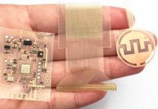
Glass PCBs are a type of substrate where the base material is made entirely or partially of glass instead of traditional epoxy or ceramic. These PCBs can be constructed using ultra-thin glass sheets, sometimes as thin as 100 micrometers, with conductive traces deposited directly onto the surface.
Key Features:
- High Thermal Stability – Glass can withstand extreme temperatures without warping.
- Excellent Dielectric Properties – Ideal for high-frequency and high-speed applications.
- Superior Dimensional Stability – Minimal expansion under heat, ensuring reliability.
- Optical Transparency – Enables applications in displays and optoelectronics.
- Chemical Resistance – Resistant to moisture and corrosive environments.
Advantages of Glass PCBs Over Traditional Materials
1. Enhanced Thermal Performance
Traditional FR4 PCBs suffer from thermal expansion, leading to reliability issues in high-power applications. Glass, with its low coefficient of thermal expansion (CTE), ensures stability even under extreme conditions, making it ideal for aerospace and automotive electronics.
2. Superior High-Frequency Performance
Glass has excellent dielectric properties, reducing signal loss at high frequencies. This makes Glass PCBs perfect for 5G communications, millimeter-wave radar, and RF applications.
3. Thinner and Lighter
Ultra-thin glass substrates allow for lighter and more compact PCB designs, crucial for wearable devices and foldable electronics.
4. Optical Applications
Transparent Glass PCBs enable integration into displays, smart windows, and biomedical sensors where visibility or light transmission is required.
5. Improved Reliability and Longevity
Glass is resistant to moisture, oxidation, and chemical degradation, ensuring longer lifespan in harsh environments.
Manufacturing Processes for Glass PCBs
Producing Glass PCBs involves several advanced techniques:
1. Glass Substrate Preparation
Ultra-thin glass sheets (e.g., Corning Willow Glass) are cleaned and treated to enhance adhesion.
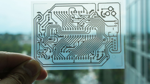
2. Conductive Patterning
- Sputtering & Evaporation – Thin metal layers (copper, gold, or silver) are deposited.
- Photolithography – A photoresist is applied, exposed to UV light, and etched to form circuits.
- Laser Direct Structuring (LDS) – Lasers selectively activate areas for metallization.
3. Lamination & Multilayer Stacking
Multiple glass layers can be bonded using adhesives or laser welding to form multilayer PCBs.
4. Via Formation
- Laser Drilling – Creates micro-vias for interlayer connections.
- Electroplating – Fills vias with conductive material.
5. Final Finishing
Surface finishes like ENIG (Electroless Nickel Immersion Gold) or OSP (Organic Solderability Preservative) are applied to protect traces.
Applications of Glass PCBs
1. High-Frequency Electronics
- 5G base stations, satellite communications, and radar systems benefit from low signal loss.
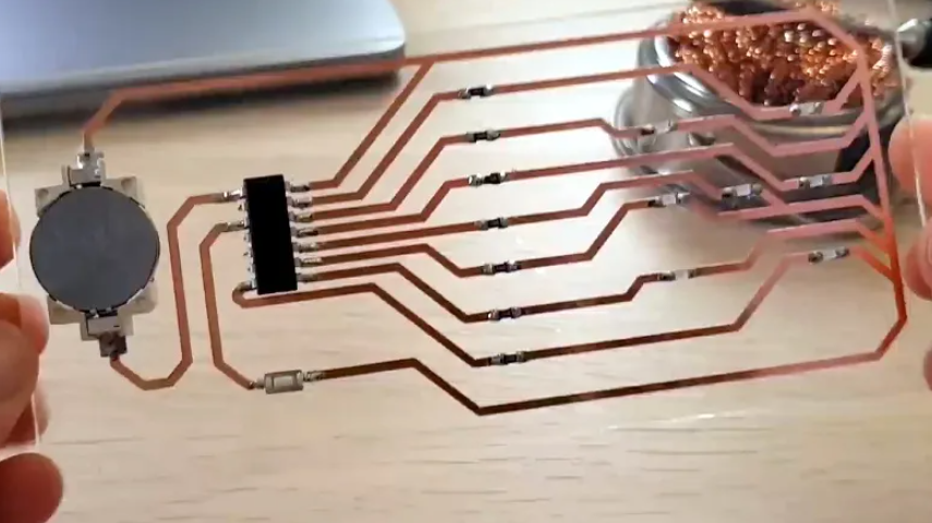
2. Flexible & Foldable Electronics
- Used in foldable smartphones, rollable displays, and wearable tech.
3. Medical Devices
- Biocompatible Glass PCBs are used in implants and diagnostic equipment.
4. Automotive & Aerospace
- Withstands high temperatures in engine control units and avionics.
5. Optoelectronics & Displays
- Transparent circuits enable smart mirrors, AR/VR devices, and OLED displays.
Challenges & Future Outlook
Current Challenges:
- Fragility – Glass is brittle, requiring careful handling.
- High Cost – Manufacturing is more expensive than FR4.
- Limited Suppliers – Few companies produce ultra-thin glass for PCBs.
Future Developments:
- Hybrid Glass-Flex PCBs – Combining flexibility with glass’s benefits.
- 3D Glass Circuitry – Enabling complex 3D-embedded electronics.
- Improved Laser Processing – Faster and more precise via drilling.
Conclusion
Glass PCBs represent a transformative shift in electronic packaging, offering unmatched thermal, electrical, and optical properties. While challenges remain in cost and fragility, ongoing advancements in material science and manufacturing techniques are paving the way for broader adoption. As industries push toward higher performance and miniaturization, Glass PCBs are poised to become a cornerstone of next-generation electronics.