The Role and Benefits of 3D Package Models in PCB Design
Introduction
In the rapidly evolving world of electronics design, printed circuit board (PCB) development has undergone significant transformations. One of the most impactful advancements in recent years has been the integration of 3D package models into the PCB design workflow. This technological shift has revolutionized how engineers approach board design, component placement, and system integration. 3D package models provide a comprehensive digital representation of electronic components, including their physical dimensions, pin configurations, and thermal characteristics. As electronic devices continue to shrink in size while increasing in complexity, the importance of accurate 3D modeling in PCB design cannot be overstated. This article explores the multifaceted role of 3D package models in modern PCB design and examines the substantial benefits they offer to design teams, manufacturers, and end products.
Enhanced Design Accuracy and Visualization
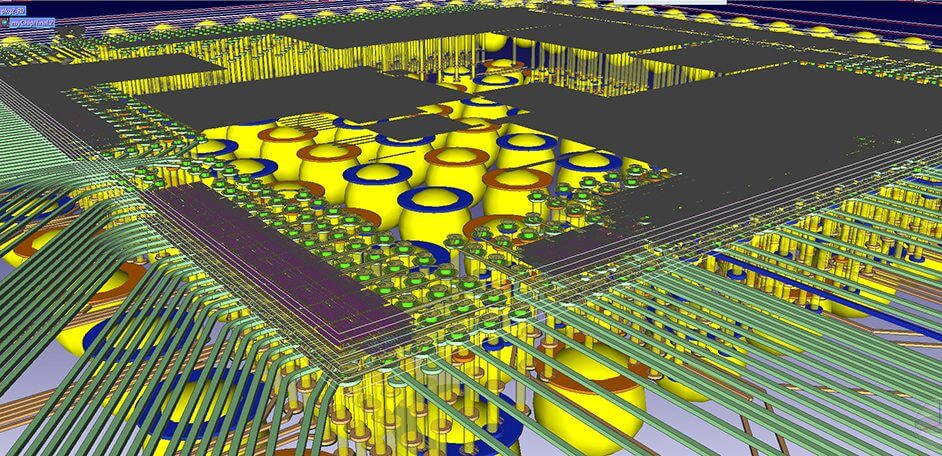
One of the primary advantages of incorporating 3D package models in PCB design is the dramatic improvement in design accuracy and visualization capabilities. Traditional 2D design approaches often led to interpretation errors and dimensional inaccuracies that might only become apparent during physical prototyping or even production. With 3D models, designers can:
- Visualize the complete board assembly in three dimensions, allowing for better spatial understanding of component placement and orientation.
- Identify potential mechanical conflicts between components, connectors, and the enclosure before prototyping.
- Verify component footprints with greater precision, reducing the risk of soldering issues during manufacturing.
- Simulate the assembly process to ensure proper clearances for automated pick-and-place machines and manual assembly.
The ability to rotate, zoom, and inspect the board from any angle provides designers with unprecedented insight into their creations, enabling them to catch potential issues early in the design cycle when changes are less costly to implement.
Improved Mechanical Integration
Modern electronic products often require tight integration between the PCB and mechanical components or enclosures. 3D package models facilitate this integration by:
- Enabling co-design between electrical and mechanical teams through seamless data exchange between ECAD and MCAD environments.
- Ensuring proper fit within enclosures by verifying clearances for mounting holes, connectors, and tall components.
- Optimizing board shape and component placement to accommodate mechanical constraints or aesthetic requirements.
- Verifying connector alignment with external interfaces and panel components.
This mechanical-electrical co-design capability significantly reduces the traditional “throw-it-over-the-wall” approach between engineering disciplines, leading to more robust product designs and fewer iterations between electrical and mechanical teams.
Thermal Management Optimization
Effective thermal management is critical for reliable electronic operation, especially in high-density designs or applications with significant power dissipation. 3D package models contribute to thermal analysis by:
- Providing accurate component geometry for computational fluid dynamics (CFD) simulations.
- Enabling visualization of heat flow across the board and through components.
- Facilitating the placement of thermal vias and heatsinks based on actual component thermal characteristics.
- Identifying potential hot spots before prototyping, allowing for proactive design changes.
By incorporating thermal information into the 3D models, designers can make informed decisions about component placement, copper pours, and board stackup to optimize heat dissipation.

Signal Integrity and EMI Analysis
High-speed digital designs and RF applications demand careful consideration of signal integrity and electromagnetic interference (EMI). 3D package models support these analyses by:
- Providing accurate representations of package parasitics that affect signal propagation.
- Enabling 3D electromagnetic field simulations to identify potential coupling issues.
- Facilitating proper grounding strategies by visualizing the complete 3D current return paths.
- Supporting antenna effect analysis for wireless devices.
These capabilities allow designers to address potential signal integrity and EMI issues early in the design process, reducing the need for costly board spins later in development.
Manufacturing and Assembly Benefits
The advantages of 3D package models extend beyond the design phase into manufacturing and assembly:
- Improved Design for Manufacturability (DFM) by identifying potential soldering or assembly issues.
- Enhanced automated optical inspection (AOI) preparation through accurate 3D reference models.
- Better process planning for pick-and-place machines and reflow oven profiles.
- Reduced manufacturing defects through comprehensive pre-production verification.
By catching potential manufacturing issues during design, companies can significantly reduce time-to-market and improve production yields.
Component Library Management
3D package models revolutionize component library management by:
- Providing a single source of truth for both electrical and mechanical properties.
- Reducing library errors through standardized, vendor-provided models.
- Facilitating component reuse across projects with confidence in mechanical compatibility.
- Enabling parametric searches based on 3D dimensions as well as electrical characteristics.
This comprehensive approach to component management reduces errors and improves design efficiency across an organization.
Collaboration and Documentation
3D models enhance collaboration and documentation through:
- Clear visual communication between team members and stakeholders.
- Accurate technical documentation with realistic illustrations.
- Improved customer presentations with photorealistic renderings.
- Better maintenance and service documentation showing exact component locations.
These benefits extend throughout the product lifecycle, from initial concept to end-of-service.
Challenges and Considerations
While 3D package models offer numerous advantages, their implementation comes with certain challenges:
- Model availability – Not all components have readily available 3D models.
- File format compatibility – Different ECAD/MCAD tools may use varying formats.
- Model accuracy – Some simplified models may lack critical details.
- Increased computational requirements – 3D operations demand more processing power.
Design teams must establish processes to address these challenges, including creating custom models when necessary and verifying model accuracy before use.
Future Trends
The use of 3D package models in PCB design continues to evolve with several emerging trends:
- Integration with augmented reality (AR) for immersive design reviews.
- Cloud-based collaboration enabling real-time 3D design sharing.
- AI-assisted model generation for components lacking official models.
- Advanced material properties in models for more accurate simulations.
These advancements promise to further enhance the benefits of 3D modeling in PCB design.
Conclusion
The incorporation of 3D package models in PCB design represents a significant leap forward in electronic product development. By providing accurate, comprehensive digital representations of components, these models enable designers to overcome many traditional challenges associated with board development. From improved visualization and mechanical integration to enhanced thermal management and signal integrity analysis, the benefits of 3D modeling permeate every aspect of the design process. Furthermore, the advantages extend into manufacturing, assembly, and product documentation, delivering value throughout the product lifecycle. As the electronics industry continues to push the boundaries of miniaturization and performance, 3D package models will undoubtedly play an increasingly vital role in ensuring successful, efficient, and cost-effective PCB design. Organizations that fully embrace this technology position themselves to achieve faster time-to-market, higher product quality, and greater innovation in their electronic designs.