The Role and Techniques of Copper Cladding in PCB Design
Introduction
Copper cladding, also known as copper pour or copper fill, is a fundamental aspect of Printed Circuit Board (PCB) design. It involves the strategic placement of copper areas on the PCB to enhance electrical performance, thermal management, and mechanical stability. This article delves into the significance of copper cladding, its various techniques, and best practices for implementation in PCB design.
1. Understanding Copper Cladding
1.1. Definition and Purpose
Copper cladding refers to the process of adding copper areas to the PCB, typically connected to a ground or power plane. The primary purpose of copper cladding is to improve the electrical conductivity, thermal dissipation, and mechanical strength of the PCB. It also helps in reducing electromagnetic interference (EMI) and providing a stable reference plane for signal integrity.
1.2. Types of Copper Cladding
There are several types of copper cladding techniques used in PCB design:
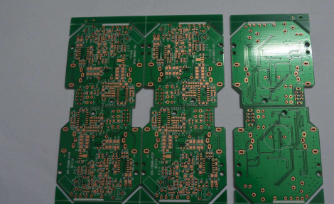
- Solid Copper Pour: This involves filling large areas of the PCB with solid copper, usually connected to a ground or power plane. It provides excellent electrical conductivity and thermal dissipation.
- Hatched Copper Pour: This technique uses a grid or hatched pattern of copper instead of a solid fill. It reduces the amount of copper used, which can help with thermal management and reduce the weight of the PCB.
- Thermal Relief Copper Pour: This involves creating small gaps or spokes in the copper pour around component pads to reduce thermal conductivity and prevent solder joint issues during reflow soldering.
2. Electrical Benefits of Copper Cladding
2.1. Improved Signal Integrity
Copper cladding plays a crucial role in maintaining signal integrity in high-speed PCB designs. By providing a continuous ground plane, copper cladding helps to reduce the impedance of the ground path, minimizing signal reflections and crosstalk. This is particularly important for high-frequency signals, where maintaining a stable reference plane is essential for signal integrity.
2.2. Reduced Electromagnetic Interference (EMI)
Copper cladding can significantly reduce electromagnetic interference (EMI) by acting as a shield that absorbs and dissipates electromagnetic radiation. The continuous copper layer creates a Faraday cage effect, preventing external electromagnetic fields from interfering with the circuit and vice versa. This is especially important in high-frequency circuits, where EMI can cause significant performance issues.
2.3. Enhanced Power Distribution
Copper cladding connected to a power plane can enhance power distribution across the PCB. By providing a low-impedance path for power delivery, copper cladding ensures that all components receive a stable and consistent power supply, reducing the risk of voltage drops and power supply noise.

3. Thermal Management Benefits
3.1. Heat Dissipation
Copper is an excellent conductor of heat, and copper cladding can significantly improve the thermal management of a PCB. By filling unused areas with copper, designers can create additional thermal pathways that help to dissipate heat away from critical components. This is particularly important for high-power circuits, where excessive heat can lead to component failure and reduced reliability.
3.2. Thermal Relief
Copper cladding can also be used to provide thermal relief for components that generate a lot of heat. Thermal relief involves creating small gaps or spokes in the copper pour around the pads of these components. This reduces the thermal conductivity between the pad and the copper pour, allowing the component to dissipate heat more effectively. Thermal relief is especially important for components that are sensitive to temperature changes, such as integrated circuits (ICs) and power transistors.
4. Mechanical Stability
4.1. Reduced Warping
Copper cladding can improve the mechanical stability of a PCB by reducing the likelihood of warping. Warping occurs when the PCB expands or contracts due to changes in temperature or humidity. By filling unused areas with copper, designers can create a more balanced and uniform distribution of material, reducing the stress on the board and minimizing the risk of warping.
4.2. Enhanced Durability
In addition to reducing warping, copper cladding can enhance the overall durability of the PCB. The additional copper provides extra structural support, making the board more resistant to mechanical stress and vibration. This is particularly important for applications where the PCB may be subjected to harsh environmental conditions, such as automotive or aerospace electronics.
5. Challenges and Considerations
5.1. Manufacturing Complexity
One of the primary challenges of copper cladding is the increased complexity it adds to the manufacturing process. The additional copper can make it more difficult to etch the board accurately, leading to potential issues with trace width and spacing. Designers must work closely with manufacturers to ensure that the copper cladding does not compromise the overall quality of the PCB.
5.2. Signal Integrity Issues
While copper cladding can improve signal integrity in many cases, it can also introduce issues if not implemented correctly. For example, if the copper cladding is too close to signal traces, it can create parasitic capacitance, leading to signal degradation. Designers must carefully consider the placement and spacing of the copper cladding to avoid these issues.
5.3. Thermal Management Challenges
While copper cladding can improve thermal management, it can also create challenges if not properly designed. For example, if the copper cladding is too thick, it can act as a heat sink, drawing heat away from critical components and reducing their effectiveness. Designers must carefully balance the thickness and placement of the copper cladding to ensure optimal thermal performance.
6. Best Practices for Implementing Copper Cladding
6.1. Proper Spacing and Clearance
One of the most important considerations when implementing copper cladding is proper spacing and clearance. Designers must ensure that the copper cladding is not too close to signal traces, as this can create parasitic capacitance and signal integrity issues. A general rule of thumb is to maintain a clearance of at least 0.2mm between the copper cladding and signal traces.
6.2. Use of Thermal Relief
As mentioned earlier, thermal relief is essential for components that generate a lot of heat. Designers should use thermal relief pads for these components to ensure that heat is dissipated effectively. This involves creating small gaps or spokes in the copper cladding around the component pads, reducing the thermal conductivity between the pad and the copper cladding.
6.3. Balanced Copper Distribution
To reduce the risk of warping and improve mechanical stability, designers should aim for a balanced distribution of copper across the PCB. This involves ensuring that the copper cladding is evenly distributed on both sides of the board and that there are no large areas of empty space. A balanced copper distribution helps to minimize stress on the board and reduce the likelihood of warping.
6.4. Consideration of Manufacturing Constraints
Designers must also consider the manufacturing constraints when implementing copper cladding. This includes working closely with the manufacturer to ensure that the copper cladding does not compromise the overall quality of the PCB. Designers should also consider the thickness of the copper cladding and its impact on the manufacturing process.
7. Conclusion
Copper cladding is a powerful technique in PCB design that offers numerous benefits, including improved electrical performance, thermal management, and mechanical stability. By filling unused areas of the PCB with copper, designers can create a more reliable and efficient circuit board. However, copper cladding also presents several challenges that must be carefully considered, including manufacturing complexity, signal integrity issues, and thermal management challenges. By following best practices and working closely with manufacturers, designers can maximize the benefits of copper cladding while minimizing potential drawbacks. As the electronics industry continues to evolve, copper cladding will remain an essential tool for creating high-performance, reliable PCBs.


