The Significance and Applications of 16 oz Copper Thickness in PCB Design
Introduction to Copper Weight in PCBs
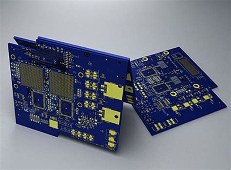
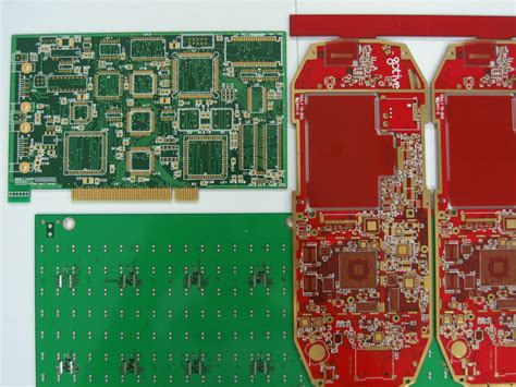
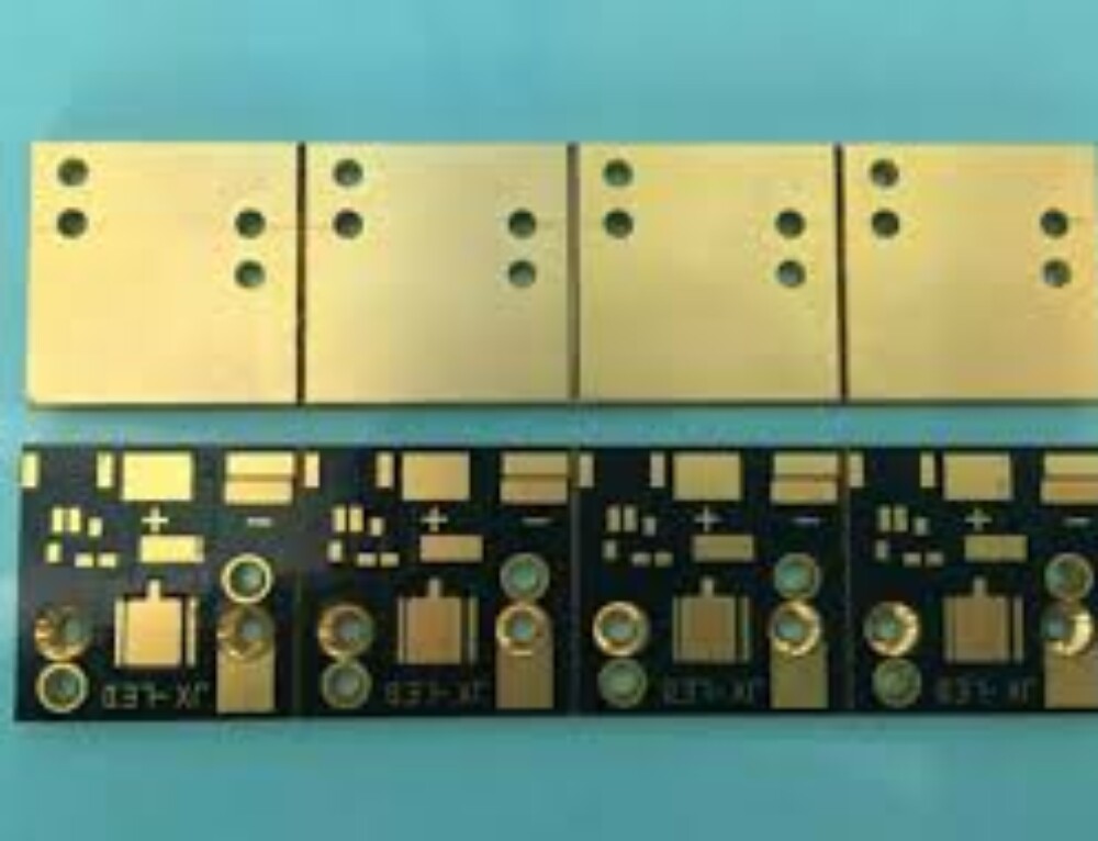
Printed Circuit Boards (PCBs) form the backbone of modern electronics, and one of their most critical characteristics is copper thickness, typically measured in ounces (oz). The 16 oz copper thickness represents one of the heaviest copper weights used in specialized PCB applications, offering unique advantages for high-power and high-current designs.
Copper weight in PCBs refers to the thickness of the copper layer laminated onto the substrate material. The “ounce” measurement comes from the weight of copper spread evenly over a one square foot area. For 16 oz copper, this translates to approximately 2.2 mils (0.0022 inches) or 56 microns in thickness—substantially thicker than standard PCB copper weights of 1 oz or 2 oz.
Understanding 16 oz Copper Specifications
Measurement and Conversion
16 oz copper represents:
- 2.2 mils (0.0022 inches) in thickness
- 56 microns (μm)
- 0.056 millimeters
This measurement applies to the copper thickness before any plating or etching processes. It’s important to note that the final thickness after manufacturing may vary slightly due to processing factors.
Comparison with Standard Copper Weights
To appreciate the substantial nature of 16 oz copper, consider these comparisons:
- Standard PCBs typically use 1 oz (1.4 mils/35 μm) or 2 oz (2.8 mils/70 μm) copper
- Heavy copper PCBs generally start at 3 oz (4.2 mils/105 μm)
- 16 oz copper is approximately 4 times thicker than standard heavy copper designs
- It represents about 11 times the thickness of standard 1 oz copper
Technical Characteristics
16 oz copper offers:
- Extremely low DC resistance (approximately 0.32 mΩ/square)
- High current-carrying capacity (upwards of 100A for typical traces)
- Excellent thermal conductivity (about 400 W/mK)
- Significant mechanical strength for structural applications
Applications of 16 oz Copper Thickness
High-Power Electronics
16 oz copper finds its primary application in high-power electronic systems:
- Power converters and inverters
- High-current bus bars and power distribution
- Electric vehicle power systems
- Industrial motor controllers
- Renewable energy systems (solar/wind power conversion)
Automotive and Transportation
The automotive industry, particularly electric vehicles, benefits from 16 oz copper PCBs:
- Battery management systems
- High-current charging circuits
- Power train control modules
- Heavy-duty electrical systems in commercial vehicles
Industrial Equipment
Industrial applications demanding robust power handling utilize 16 oz copper:
- Welding equipment
- Large motor drives
- Power supplies for industrial machinery
- High-power RF amplifiers
Aerospace and Defense
Critical aerospace systems employ 16 oz copper for:
- Power distribution in aircraft
- Radar and communication systems
- Military-grade power electronics
- Satellite power systems
Unique Applications
Specialized uses include:
- High-power LED arrays
- Power electronics for scientific equipment
- Custom bus bar replacements
- High-frequency trading server power systems

Advantages of 16 oz Copper Thickness
Current Carrying Capacity
The primary advantage of 16 oz copper is its exceptional current-carrying capacity:
- Can handle currents up to 100A or more in properly designed traces
- Reduces current density, minimizing resistive heating
- Allows for shorter, more compact power paths compared to thinner copper
Thermal Management
16 oz copper provides outstanding thermal performance:
- Acts as an effective heat spreader, dissipating heat from components
- Reduces hot spots in high-power designs
- Can often eliminate or reduce the need for additional heat sinks
- Maintains lower operating temperatures for improved reliability
Mechanical Strength
The substantial copper layer offers:
- Enhanced board rigidity and durability
- Resistance to mechanical stress and vibration
- Better performance in high-vibration environments
- Improved structural integrity for large or heavy components
Design Flexibility
Engineers gain design advantages:
- Ability to create custom in-plane bus bars
- Reduced need for external wiring in power circuits
- More compact power circuit layouts
- Integration of high-power and control circuits on single board
Reliability and Longevity
16 oz copper enhances product reliability:
- Reduced electromigration effects
- Lower thermal cycling stress
- Improved resistance to power surges
- Longer operational life in demanding conditions
Design Considerations for 16 oz Copper PCBs
Trace and Space Requirements
Designing with 16 oz copper presents unique challenges:
- Minimum trace widths are significantly larger than standard PCBs
- Typical minimum trace/space rules start at 0.020″ (20 mils) or more
- Aspect ratio concerns with thick copper in relation to dielectric thickness
- Increased need for teardrops and pad reinforcements
Etching Challenges
The etching process requires special consideration:
- Longer etch times required for thick copper
- Potential for undercutting if not properly controlled
- Need for specialized etchants and processes
- Increased difficulty in maintaining fine feature accuracy
Plating Considerations
Plated through-holes in 16 oz boards need attention:
- Ensuring sufficient plating thickness in holes
- Managing copper distribution during plating
- Potential for uneven plating in high-aspect ratio holes
- Special attention to annular ring requirements
Thermal Management Design
While 16 oz copper helps thermal performance, designers must:
- Consider thermal expansion differences
- Plan for proper heat dissipation paths
- Account for potential warpage from copper weight
- Design appropriate thermal relief patterns
Manufacturing Tolerances
Expect wider tolerances with 16 oz copper:
- Increased variation in final copper thickness
- Greater potential for impedance variations
- More significant dimensional changes during processing
- Need for closer communication with fabricators
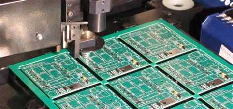
Manufacturing Processes for 16 oz Copper PCBs
Material Selection
Key material considerations include:
- High-temperature laminates to withstand processing
- Materials with good dimensional stability
- Substrates with appropriate thermal expansion characteristics
- Prepregs capable of filling heavy copper features
Specialized Imaging
The photolithography process requires:
- Thick photoresist applications
- High-resolution exposure systems
- Careful alignment procedures
- Potential for multiple imaging steps
Etching Techniques
Fabricators employ specialized etching:
- Differential etching techniques
- Controlled etch rate processes
- Potential for stepped etching
- Advanced etch chemistry management
Plating Processes
Plating 16 oz boards involves:
- Extended plating cycles
- High-throw plating solutions
- Potential for pulse plating techniques
- Careful monitoring of plating uniformity
Quality Control
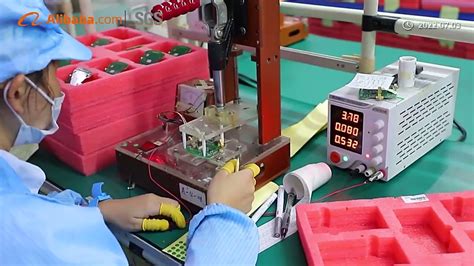
Enhanced QC measures include:
- Cross-section analysis
- Microsectioning for thickness verification
- Enhanced automated optical inspection
- Rigorous electrical testing
Challenges and Limitations
Fabrication Complexity
16 oz copper PCBs present manufacturing challenges:
- Limited number of capable fabricators
- Significantly higher production costs
- Longer lead times compared to standard PCBs
- Increased potential for yield issues
Design Restrictions
Engineers face design constraints:
- Limited ability to create fine features
- Reduced routing density
- Challenges with high-density interconnects
- Restrictions on layer count in multilayer designs
Cost Considerations
Economic factors include:
- Material costs substantially higher than standard PCBs
- Increased processing costs
- Potential for higher scrap rates
- Need for specialized equipment investment
Availability Issues
Potential supply chain challenges:
- Limited laminate material options
- Fewer capable PCB manufacturers
- Longer procurement timelines
- Potential for minimum order quantities
Future Trends in Heavy Copper PCBs
Technology Advancements
Emerging developments include:
- Improved etching techniques for better precision
- Advanced plating methods for uniform coverage
- New laminate materials supporting heavier copper
- Enhanced thermal management solutions
Growing Applications
Expanding uses in:
- Electric vehicle power systems
- Renewable energy infrastructure
- High-power computing
- 5G infrastructure power delivery
Material Innovations
Future material developments may bring:
- Composite copper materials for better performance
- Advanced dielectric materials for heavy copper
- Nano-structured copper for improved properties
- Hybrid copper-aluminum solutions
Conclusion
16 oz copper thickness represents a specialized but critical solution in the PCB industry, addressing the demanding requirements of high-power electronic applications. While presenting unique design and manufacturing challenges, its exceptional current-carrying capacity, thermal performance, and mechanical strength make it indispensable for certain applications.
As power demands continue to grow across industries from automotive to renewable energy, the importance of heavy copper solutions like 16 oz will only increase. Engineers working with high-power designs must understand both the capabilities and limitations of this technology to effectively incorporate it into their products.
The future of 16 oz copper PCBs looks promising, with ongoing advancements in materials and manufacturing processes continually expanding their potential applications while addressing current limitations. For applications where extreme power handling is required, 16 oz copper remains an essential tool in the electronics designer’s toolkit.