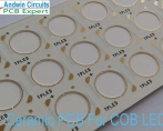
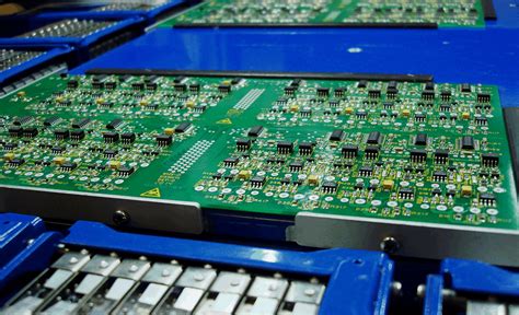
The summarize of high precision technology print PCB
High-precision printed circuits refer to the use of fine line width/spacing, micro-holes, narrow ring width (or no ring width) and buried and blind vias to achieve high density. High precision means “fine, small, narrow, thin”, which will inevitably lead to high precision requirements. Take line width as an example: 0.20mm line width, according to regulations, 0.16~0.24mm is qualified, and its error is (0.20±0.04)mm; and 0.10mm line width, similarly, its error is (0.10±0.02)mm.
Obviously, the latter has doubled its accuracy, and so on. Therefore, high-precision requirements are no longer discussed separately. However, it is a prominent problem in production technology
(1) Fine wire technology In the future, high-fine line width/spacing will be from 0.20mm-0.13mm-0.08mm to 0.005mm to meet the requirements of SMT and multi-chip packaging (Multichip Package, MCP) requirements. Therefore, the following technologies are required.
① Use thin or ultra-thin copper foil (<18um) substrate and fine surface treatment technology.
② Use thinner dry film and wet film lamination process. Thin and high-quality dry film can reduce line width distortion and defects. Wet film lamination can fill small air gaps, increase interface adhesion, and improve wire integrity and precision.
③ Use electro-deposited photoresist (ED). Its thickness can be controlled in the range of 5~30/um, which can produce more perfect fine wires. It is particularly suitable for narrow ring width, no ring width and full board electroplating. There are more than ten ED production lines in the world.
④Use parallel light exposure technology. Since parallel light exposure can overcome the influence of line width variation caused by the oblique light rays of the “point” light source, fine wires with precise line width and smooth edges can be obtained. However, parallel exposure equipment is expensive, requires high investment, and requires working in a high-cleanliness environment.
⑤Use automatic optical inspection technology (Automatic Optic Inspection, AOI). This technology has become an essential means of inspection in the production of fine wires and is being rapidly promoted, applied and developed. For example, AT&T has 11 AoIs, and Tadco has 21 AoIs specifically used to inspect the inner layer graphics.
(2) Micro-hole technology The functional holes of printed circuit boards for surface mounting are mainly used for electrical interconnection,
which makes the application of micro-hole technology more important. The use of conventional drill materials and CNC drilling machines to produce micro-holes has many faults and high costs. Therefore, the high-density of printed circuit boards is mostly achieved by focusing on the fineness of wires and pads. Although great achievements have been made, its potential is limited. To further improve the fineness (such as wires less than 0.08mm), the cost will rise sharply, so micro-holes are used to improve the fineness.
In recent years, CNC drilling machines and micro-drill technology have made breakthrough progress, so micro-hole technology has developed rapidly. This is the main outstanding feature of current printed circuit board production. In the future, micro-hole formation technology will mainly rely on advanced CNC drilling machines and excellent micro-heads, and the small holes formed by laser technology are still inferior to those formed by CNC drilling machines from the perspective of cost and hole quality.
① CNC drilling machine At present, the technology of CNC drilling machines has made new breakthroughs and progress.
A new generation of CNC drilling machines with the characteristics of drilling tiny holes has been formed. The efficiency of micro-hole drilling machines in drilling small holes (less than 0.50mm) is 1 times higher than that of conventional CNC drilling machines, with fewer failures and a rotation speed of 11~15r/min; it can drill 0.1~0.2mm micro-holes, use high-quality small drill bits with high cobalt content, and can stack three plates (1.6mm/piece) for drilling. If the drill bit breaks, it can automatically stop and report the position, automatically replace the drill bit and check the diameter (the tool library can hold hundreds of drill bits), and can automatically control the constant distance between the drill tip and the cover plate and the drilling depth, so it can drill blind holes without damaging the table top. The CNC drilling machine table uses air cushion and magnetic levitation, which moves faster, lighter, more accurately, and will not scratch the table top. Such drilling machines are currently in short supply, such as the Mega 4600 of Prurite in Italy and the ExcelIon of the United States. 2000 series, as well as new generation products from Switzerland, Germany, etc.
② Laser drilling. Conventional CNC drilling machines and drills for drilling micro-holes do have many problems.
This has hindered the progress of micro-hole technology, so laser hole etching has received attention, research and application. However, there is a fatal disadvantage, that is, the formation of horn holes, which becomes more serious as the thickness of the board increases. In addition, the pollution of high-temperature ablation (especially multi-layer boards), the life and maintenance of the light source, the repetitive accuracy of the hole etching and the cost, etc., have limited the promotion and application of micro-holes in the production of printed circuit boards. However, laser hole etching is still used in thin and high-density micro-hole boards, especially in the high-density interconnection (HDI) technology of MCM-L, such as the high-density interconnection of polyester film hole etching and metal deposition (sputtering technology) in M.C.Ms. It can also be used in the formation of buried holes in high-density interconnected multi-layer boards with buried and blind hole structures. However, due to the development of CNC drilling machines and micro-drills and technological breakthroughs, it has been rapidly promoted and applied. Therefore, laser drilling on the surface
The application of installing printed circuit boards cannot form a dominant position. But it still has a place in a certain field.
③ Buried, blind, and through-hole technology Buried, blind, and through-hole combination technology is also an important way to improve the high density of printed circuits.
Generally, buried and blind holes are tiny holes. In addition to increasing the number of wiring on the board, buried and blind holes use the “closest” inner layer interconnection, which greatly reduces the number of through-holes formed, and the isolation plate setting will also be greatly reduced, thereby increasing the number of effective wiring and interlayer interconnection in the board, and improving the high density of interconnection. Therefore, the multi-layer board with buried, blind, and through-hole combination has a higher interconnection density than the conventional full-through-hole board structure under the same size and number of layers.
At least 3 times higher. If the same technical indicators are used, the size of the printed circuit board with buried, blind and through holes will be greatly reduced or the number of layers will be significantly reduced. Therefore, in high-density surface-mounted printed circuit boards, buried and blind hole technology has been increasingly used. It is not only used in surface-mounted printed circuit boards in large computers and communication equipment, but also widely used in civil and industrial fields, and even in some thin boards, such as various PCMCIA, Smard, IC cards, etc. Thin six-layer boards.
Printed circuit boards with buried and blind hole structures are generally produced by “separating boards”, which means that they must be completed after multiple pressing, drilling, hole plating, etc., so precise positioning is very important.