The Three Major Factors Affecting PCB Impedance Control
Abstract
Impedance control is critical in modern printed circuit board (PCB) design, especially for high-speed digital and RF applications. Precise impedance matching ensures signal integrity, minimizes reflections, and reduces electromagnetic interference (EMI). This article explores the three primary factors influencing PCB impedance: trace geometry, dielectric material properties, and reference plane configuration. Understanding these factors helps designers optimize PCB layouts for high-frequency performance.
1. Introduction
As signal frequencies increase in modern electronics, maintaining controlled impedance in PCB traces becomes essential. Mismatched impedance leads to signal degradation, data errors, and system failures. The characteristic impedance of a transmission line on a PCB depends on several physical and material properties. The three most significant factors are:
- Trace Geometry (width, thickness, and spacing)
- Dielectric Material Properties (permittivity, thickness, and consistency)
- Reference Plane Configuration (ground/power plane placement and return paths)
This article examines each factor in detail, providing insights into how designers can achieve optimal impedance control.
2. Trace Geometry
The physical dimensions of PCB traces directly impact impedance. Key parameters include trace width, thickness, and spacing from other conductors.
2.1 Trace Width
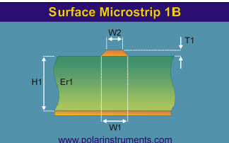
Impedance is inversely proportional to trace width—wider traces reduce impedance, while narrower traces increase it. For microstrip traces (surface-level routing), the relationship can be approximated using empirical formulas:
[Z_0 \approx \frac{87}{\sqrt{\varepsilon_r + 1.41}} \ln \left( \frac{5.98h}{0.8w + t} \right)]
Where:
- ( Z_0 ) = Characteristic impedance (Ω)
- ( \varepsilon_r ) = Dielectric constant
- ( h ) = Dielectric height (substrate thickness)
- ( w ) = Trace width
- ( t ) = Trace thickness
Designers must carefully select trace widths based on target impedance, manufacturing tolerances, and current-carrying requirements.
2.2 Trace Thickness
Thicker traces (e.g., 2 oz copper vs. 1 oz copper) decrease impedance due to increased cross-sectional area. However, etching tolerances can affect precision, leading to variations in impedance.
2.3 Spacing Between Traces (Differential Pairs)
For differential signaling (e.g., USB, PCIe), the spacing between paired traces affects differential impedance. Tight coupling (small spacing) increases mutual capacitance and reduces impedance, while wider spacing reduces coupling and raises impedance.
3. Dielectric Material Properties
The PCB substrate’s dielectric properties significantly influence impedance. The key parameters are dielectric constant (( \varepsilon_r )) and dielectric thickness.
3.1 Dielectric Constant (( \varepsilon_r ))
The dielectric constant (Dk) determines how much the electric field is concentrated in the substrate. Higher ( \varepsilon_r ) lowers impedance because the electric field is more confined. Common PCB materials include:
- FR4 (( \varepsilon_r \approx 4.2 – 4.8 ))
- Rogers RO4350B (( \varepsilon_r \approx 3.48 ))
- Isola I-Tera (( \varepsilon_r \approx 3.45 ))
High-frequency designs often use low-Dk materials to minimize signal loss and dispersion.
3.2 Dielectric Thickness
Thicker dielectrics increase impedance by reducing capacitive coupling between the trace and reference plane. Stripline configurations (traces embedded between two planes) are more sensitive to dielectric thickness than microstrips.
3.3 Dielectric Consistency
Variations in dielectric thickness or ( \varepsilon_r ) across the PCB (due to manufacturing tolerances or moisture absorption) can cause impedance mismatches. High-quality laminates with tight tolerances are essential for controlled impedance.
4. Reference Plane Configuration
The return path for high-frequency signals is critical for impedance control. The presence and positioning of reference (ground/power) planes affect impedance stability.
4.1 Proximity of Reference Planes
A closer reference plane reduces impedance by increasing capacitive coupling. In microstrip designs, the distance to the ground plane (( h )) is a key variable. Stripline designs (traces between two planes) provide better impedance consistency but require precise layer stackup control.
4.2 Return Path Discontinuities
Gaps, splits, or voids in reference planes disrupt return currents, causing impedance variations and signal reflections. Designers must ensure uninterrupted return paths beneath critical traces.
4.3 Plane Material and Conductivity
While most PCBs use copper planes, variations in surface roughness or plating can slightly affect impedance. Electrodeposited (ED) copper vs. rolled copper can exhibit different high-frequency characteristics.
5. Practical Considerations for PCB Design
To achieve consistent impedance control, designers should:
- Use impedance calculators (e.g., Polar SI9000) or field solvers for accurate modeling.
- Work closely with PCB manufacturers to account for process variations.
- Perform signal integrity simulations (e.g., HyperLynx, ADS) before fabrication.
- Test impedance using TDR (Time Domain Reflectometry) measurements.
6. Conclusion
Controlled impedance is vital for high-speed PCB designs, and the three major influencing factors—trace geometry, dielectric properties, and reference plane configuration—must be carefully optimized. By understanding these variables, engineers can design PCBs with minimal signal distortion, ensuring reliable performance in modern electronic systems.