The Top 3 Causes of PCB Via Plugging Failures and Effective Solutions
Introduction
Printed Circuit Boards (PCBs) are essential components in modern electronics, and via plugging (via filling) is a critical process that ensures reliable electrical connections and structural integrity. However, via plugging defects can lead to poor conductivity, solder voids, and even PCB failure.
This article explores the top 3 causes of PCB via plugging failures and provides practical solutions to improve manufacturing quality.
1. Insufficient Via Filling Material
Problem:
One of the most common causes of poor via plugging is inadequate filling material, leading to voids, incomplete filling, or uneven distribution. This issue arises due to:
- Low-viscosity plugging ink that flows out before curing
- Improper stencil design leading to insufficient material deposition
- Air bubbles trapped inside the via during filling
Consequences:
- Solder leakage during reflow soldering
- Weak mechanical strength, increasing the risk of via cracking
- Poor electrical conductivity due to incomplete filling
Solutions:
✔ Optimize Plugging Ink Viscosity – Use high-thixotropy ink to prevent sagging and ensure complete filling.
✔ Adjust Stencil Design – Increase stencil thickness or aperture size to deposit more material.
✔ Vacuum-Assisted Filling – Apply vacuum pressure during filling to remove trapped air bubbles.
✔ Multiple Filling & Curing Steps – Fill vias in two passes to ensure complete coverage before final curing.

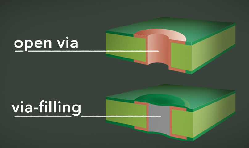
2. Poor Plating Coverage in Via Holes
Problem:
Electroplating defects inside vias can lead to weak interconnections or open circuits. Common plating issues include:
- Incomplete copper deposition due to poor hole wall preparation
- Over-etching causing thin or uneven plating layers
- Electroplating voids from contamination or improper current density
Consequences:
- Increased resistance, leading to signal loss
- Thermal stress failures due to weak plating
- Corrosion susceptibility in humid environments
Solutions:
✔ Improve Desmear & Hole Cleaning – Use plasma treatment or chemical desmear to enhance adhesion.
✔ Optimize Electroplating Parameters – Adjust current density, bath chemistry, and agitation for uniform plating.
✔ Implement Pulse Plating – Reduces voids by improving copper distribution.
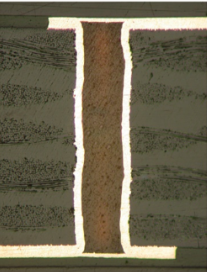
✔ Conduct Microsection Analysis – Regularly inspect via cross-sections to detect plating defects early.
3. Improper Curing of Plugging Material
Problem:
If the plugging material (e.g., epoxy, conductive ink) is not cured properly, it can lead to:
- Soft or sticky residues inside vias
- Shrinkage cracks after reflow soldering
- Delamination from via walls
Root Causes:
- Insufficient curing temperature or time
- Moisture absorption before curing
- Incompatible curing profiles for different materials
Consequences:
- Solder ball formation during assembly
- Reduced adhesion strength, causing via failure under thermal stress
- Outgassing, leading to blowholes in soldered joints
Solutions:
✔ Follow Manufacturer’s Curing Guidelines – Ensure proper time, temperature, and ramp rates.
✔ Pre-Baking to Remove Moisture – Dry PCBs at 100–120°C before plugging to prevent voids.
✔ Use UV + Thermal Dual Curing – Enhances polymerization for deeper via filling.
✔ Implement In-Line Inspection – Use AOI (Automated Optical Inspection) to detect uncured material.
Conclusion: Best Practices to Prevent Via Plugging Failures
To minimize PCB via plugging defects, manufacturers should:
- Select high-quality plugging materials with optimal viscosity and curing properties.
- Optimize plating processes to ensure uniform copper coverage.
- Implement strict curing controls to avoid shrinkage and delamination.
- Conduct regular inspections (microsection analysis, AOI, X-ray) to detect defects early.
By addressing these three major causes—insufficient filling, poor plating, and improper curing—PCB manufacturers can significantly improve via reliability, yield rates, and product performance.
Final Thoughts
Via plugging defects can be costly, but with proper process controls and material selection, they can be effectively mitigated. Implementing these solutions will lead to higher-quality PCBs with improved durability and electrical performance.
Would you like a more detailed analysis on any specific aspect of PCB manufacturing? Let me know how I can assist further! 🚀