The Ubiquitious “City Skeleton”:Unveiling the PCB,the Mysterious Map of the Electronic world”
Have you ever wondered what’d inside when you scroll through your phone screen,tap on your computer keyboard,or turn on your smart TV?Take apart any electronic device ,and you likely won’t see a tangles mess of wires.Instead,you’ll see a green board covered in silver lines and a variety of”small building block.”
This board is the “skeleton”and nervous system”of modern electronic devices-the PCB.Today .Let’s unveil its mysteries.
1.What is a PCB?
PCB,short for”Printed Circuit Board” is also more commonly known as”Circuit board”
You can think of it as a meticulously planned”miniature city”:
“Substrate”:The green baseboard,typically made of fiberglass and epoxy resin,acts as the city”foundation”,providing both strength and insulation.
“Wires”:The gleaming silver lines on the board are the city’s “road system”.They are responsible for accurately transporting electrical current and signals to their respective destinations.
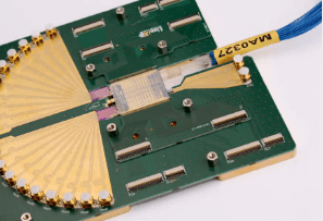
“Electronic components”:Those variously shaped”building blocks”soldered onto circuit board(such as chips,resistors,capacitors,and LED)are the “functional building”of a city,such as homes,factories ,and power plants each fulfilling a distinct role.
“Pads”:The silver dots that connect components and wires are like the entrances and exits or parking lots connecting roads to buildings.
“Vias”:The tiny holes in circuit boards are like the”overpasses”or”underground tunnels”of a city,connecting different levels of wiring.
Without PCBs,these electronic components cannot be connected and function together in an orderly manner.Therefore,PCBs are known as the “mother of electronic products”and are indispensable to almost all electronic devices.
2.How are PCBs manufactured?
The creation of a PCB is complex and sophisticated process that can be summarized in the following steps:
(1)Design:Using Software to ”Draw the Map”
Engineers use professional EDA software to design the”blueprint”of the PCB based on the circuit’s functionality.This blueprint defines the routing of all wires,the Placement of components,and the structure of each layer.
(2)PCB Fabrication:From “Baseboard”to”Engraving Circuits”
First,prepare a copper-clad board-a substrate covered with a thin layer of copper foil.
Then,using a technique similar to film exposure,the designed circuit diagram is transferred to the copper-clad board.The copper foil is protected where exposed to light.
Next,the board is placed in an etching solution,which corrodes away the unprotected copper foil while leaving the protected areas,forming the silvery traces we see.This process is like a sculptor carving a path into a copper plate.
(3) “Drilling and Plating”
Precision drills are used to create vias where connection are needed .A layer of metal is then plated on the inside of the holes,allowing interconnection between circuits on different layers.
(4)Solder Mask and Silkscreen
Apply that familiar green(or other color like blue,red or black)paint-this is the solder mask.Its function is to prevent accidental short circuits between wires during soldering and protect the circuits from oxidation and damage.
Finally,white text and symbols(silkscreen)are printed on the board to indicate component location and orientation,making assembly and maintenance easier for engineers.
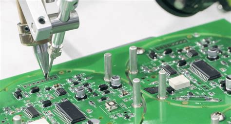
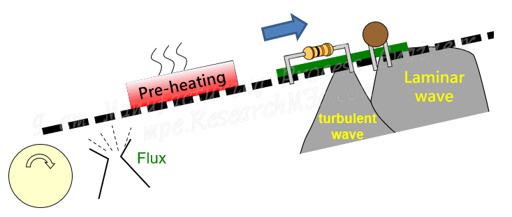
(5)Component Assembly
An automated machine(such as placement machine)precisely places the tiny electronic components on the corresponding positions on the board.High-temperature soldering secures them to the PCB.This completes the circuit board.
3.What are the types of PCBs?
PCBs are categorized by complexity:
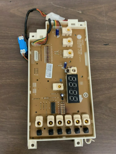
“Single-sided board:”The simplest type,with circuity on only one side of the substrate Circuitry is often found in old radios and rice cookers.
“Double-sided board”Circuitry is distributed on both sides of the most common and widely used type.
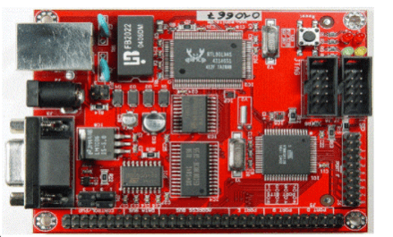
“Multi-layer board”:Like a sandwich cookie,it is made up of multiple layers of single-or double-sided boards laminated together,with precise interconnections between layers vias.High-performance devices like mobile phones and computer motherboards all use multilayer boards(typically 4-12 layers,or even more),which enable extremely complex wiring within limited space.
4.Why are PCBs important?
(1)High Reliability:Produced through rigorous industrial processes,they avoid the errors that can occur with manual wiring and offer exceptional stability.
(2)High Density and Miniaturization:They enable powerful portable devices like smart phones and smart twatches.
(3)Mass producibility:Once a design is finalized they can be quickly and cost-effectively replicated on a large scale.
(4)Easy Maintenance and debugging:Standardized designs and clear silkscreen printing make fault diagnosis and repair relatively easy.
Conclusion
From home appliances to spacecraft,from the smartphone in your hand to the servers that power the global internet.PCBs are ubiquitous.Though unseen,hidden with devices,they are the cornerstone and arteries of the entire electronic world.
The next time you use an electronic device,imagine that beneath its exquisite shell,there is a vibrant and orderly miniature city built of PCBs running efficiently .It is this city that transforms codes and instructions into the wonderful digital world that we can see and touch.