Thermal relief pad pcb
Importance Of Thermal Relief Pad PCB Design
In the realm of printed circuit board (PCB) design, thermal management is a critical aspect that can significantly influence the performance and reliability of electronic devices.
One of the essential components in this context is the thermal relief pad.
These pads play a pivotal role in ensuring that heat generated by electronic components is effectively dissipated, thereby maintaining the integrity and functionality of the PCB.
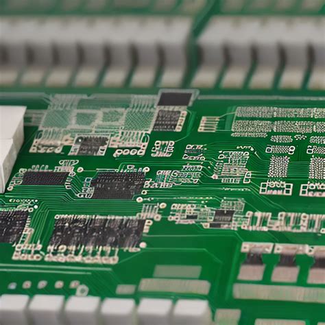
Thermal relief pads are specially designed areas on a PCB that facilitate the transfer of heat away from heat-sensitive components. They are typically used in conjunction with vias, which are small holes that allow for electrical connections between different layers of the PCB. By providing a controlled path for heat to travel, thermal relief pads help to prevent localized overheating, which can lead to component failure or reduced lifespan.
The importance of thermal relief pads becomes evident when considering the thermal dynamics within a PCB.
Electronic components, especially those with high power consumption, generate significant amounts of heat during operation. If this heat is not adequately managed, it can accumulate and cause the temperature of the PCB to rise to levels that may compromise the performance of the components. Thermal relief pads mitigate this risk by providing a means for heat to be conducted away from the components and dissipated into the surrounding environment.
Moreover, thermal relief pads are crucial in maintaining the mechanical stability of the PCB. Excessive heat can cause thermal expansion, leading to warping or delamination of the board. This not only affects the physical structure of the PCB but can also disrupt the electrical connections, resulting in intermittent or permanent failures. By incorporating thermal relief pads, designers can ensure that the thermal stresses are evenly distributed, thereby preserving the structural integrity of the PCB.
In addition to their role in heat dissipation, thermal relief pads also facilitate the soldering process during PCB assembly.
When components are soldered onto a PCB, the heat from the soldering iron must be sufficient to melt the solder and create a reliable electrical connection. However, if the heat is conducted away too quickly, it can result in cold solder joints, which are weak and prone to failure. Thermal relief pads provide a controlled thermal path that allows for efficient soldering while preventing excessive heat loss.
Furthermore, the design and placement of thermal relief pads require careful consideration to optimize their effectiveness.
Factors such as the size and shape of the pads, the number and distribution of vias, and the thermal conductivity of the materials used all play a role in determining the efficiency of heat dissipation. Advanced simulation tools and thermal analysis software are often employed to model the thermal behavior of the PCB and identify the optimal configuration for thermal relief pads.
In conclusion, thermal relief pads are indispensable in PCB design, serving multiple functions that enhance the performance, reliability, and longevity of electronic devices. By providing a controlled pathway for heat dissipation, they prevent overheating, maintain mechanical stability, and facilitate efficient soldering. As electronic devices continue to become more powerful and compact, the importance of effective thermal management through the use of thermal relief pads will only continue to grow. Therefore, designers must give due consideration to the incorporation of these pads in their PCB layouts to ensure the successful operation of their electronic products.
How To Optimize Thermal Relief Pads For Efficient Heat Dissipation
Thermal relief pads play a crucial role in printed circuit board (PCB) design, particularly in managing heat dissipation. Efficient heat management is essential to ensure the longevity and reliability of electronic components. To optimize thermal relief pads for efficient heat dissipation, several factors must be considered, including pad design, material selection, and layout strategies.
Firstly, the design of thermal relief pads significantly impacts their effectiveness.
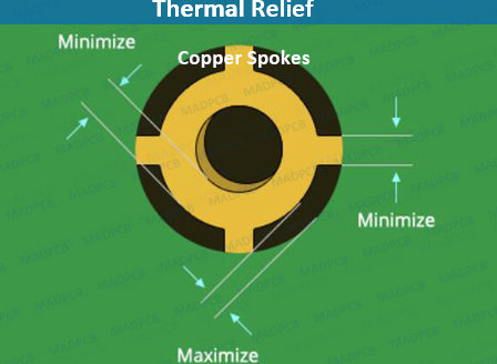
These pads are typically used to connect thermal vias to ground or power planes, allowing heat to be conducted away from heat-generating components. The geometry of the thermal relief pad, including the number and width of the spokes, is critical. A common design includes four spokes, which provide a balance between electrical connectivity and thermal isolation. However, the width of these spokes should be carefully chosen; wider spokes enhance thermal conductivity but may compromise electrical isolation, while narrower spokes improve isolation but reduce thermal conductivity. Therefore, a balanced approach is necessary to achieve optimal performance.
In addition to pad design, the choice of materials is paramount.
The thermal conductivity of the PCB substrate and the copper layers directly influences heat dissipation. High thermal conductivity materials, such as aluminum or copper-clad laminates, are preferred for applications requiring efficient heat management. These materials facilitate the rapid transfer of heat away from critical components, thereby preventing overheating. Moreover, the thickness of the copper layers also plays a role; thicker copper layers can dissipate more heat but may increase the overall cost and weight of the PCB. Thus, selecting the appropriate material and copper thickness is essential for optimizing thermal relief pads.
Furthermore, the layout of the PCB can significantly affect thermal performance. Strategic placement of thermal vias and relief pads can enhance heat dissipation.
Thermal vias are vertical pathways that connect different layers of the PCB, allowing heat to be transferred from the surface to the inner layers or to an external heat sink. Placing thermal vias directly beneath heat-generating components and connecting them to thermal relief pads can create an efficient heat dissipation pathway. Additionally, distributing thermal vias evenly across the PCB can prevent localized hotspots and ensure uniform heat distribution.
Another important consideration is the use of thermal management software during the design phase.
These tools can simulate the thermal behavior of the PCB, allowing designers to identify potential issues and optimize the placement of thermal relief pads and vias. By analyzing the thermal profile of the PCB, designers can make informed decisions about pad geometry, material selection, and layout strategies. This proactive approach can significantly enhance the thermal performance of the final product.
Moreover, it is essential to consider the operational environment of the PCB.
Factors such as ambient temperature, airflow, and the presence of external heat sinks can influence the effectiveness of thermal relief pads. For instance, in high-temperature environments, additional cooling mechanisms, such as fans or heat sinks, may be necessary to complement the thermal relief pads. Understanding the operational conditions allows designers to tailor their thermal management strategies accordingly.
In conclusion, optimizing thermal relief pads for efficient heat dissipation involves a multifaceted approach that includes careful pad design, material selection, strategic layout, and the use of thermal management software. By considering these factors, designers can enhance the thermal performance of PCBs, ensuring the reliability and longevity of electronic components. This holistic approach to thermal management is essential in the development of high-performance electronic devices.
Common Mistakes To Avoid When Designing Thermal Relief Pads
When designing thermal relief pads for printed circuit boards (PCBs), it is crucial to avoid common mistakes that can compromise the functionality and reliability of the final product. One of the most frequent errors is the improper sizing of thermal relief pads. Designers often either make the pads too large or too small, which can lead to inefficient heat dissipation or difficulty in soldering components. To mitigate this, it is essential to adhere to industry standards and guidelines, ensuring that the thermal relief pads are appropriately sized for the specific application.
Another common mistake is neglecting the thermal conductivity of the materials used.
The choice of materials significantly impacts the thermal performance of the PCB. For instance, using a material with low thermal conductivity can result in inadequate heat dissipation, leading to overheating and potential failure of electronic components. Therefore, it is imperative to select materials with high thermal conductivity to enhance the efficiency of thermal relief pads.
In addition to material selection, the placement of thermal relief pads is a critical factor that designers often overlook.
Incorrect placement can lead to uneven heat distribution, causing hotspots and thermal stress on certain areas of the PCB. To avoid this, designers should strategically place thermal relief pads in locations that promote even heat distribution across the board. This involves careful planning and simulation to identify potential problem areas and address them during the design phase.
Furthermore, the number of thermal relief pads used can also impact the overall thermal management of the PCB.
Using too few pads can result in insufficient heat dissipation, while using too many can complicate the manufacturing process and increase costs. Striking a balance is key, and this requires a thorough understanding of the thermal requirements of the PCB and the components it houses. By conducting thermal analysis and simulations, designers can determine the optimal number of thermal relief pads needed to achieve efficient heat management.
Another pitfall to avoid is the improper connection of thermal relief pads to the ground plane.
A common mistake is to connect the pads directly to the ground plane without considering the thermal resistance. This can lead to poor thermal performance and increased thermal resistance, which can adversely affect the PCB’s reliability. To address this, designers should use thermal vias to connect the thermal relief pads to the ground plane, thereby reducing thermal resistance and improving heat dissipation.
Moreover, it is essential to consider the impact of thermal relief pads on the electrical performance of the PCB.
Improper design can lead to increased electrical resistance, which can affect signal integrity and overall performance. To avoid this, designers should ensure that the thermal relief pads are designed to minimize electrical resistance while still providing adequate thermal management. This involves careful consideration of the pad geometry and the use of appropriate design tools to optimize both thermal and electrical performance.
Lastly, it is important to conduct thorough testing and validation of the thermal relief pad design.
Relying solely on simulations and theoretical calculations can lead to unforeseen issues during the manufacturing and operational phases. By conducting real-world testing and validation, designers can identify and address any potential problems, ensuring that the final product meets the required thermal and electrical performance standards.
In conclusion, avoiding common mistakes in the design of thermal relief pads for PCBs is essential for ensuring efficient heat management and reliable performance. By paying attention to pad sizing, material selection, placement, number of pads, connection to the ground plane, and electrical performance, designers can create effective thermal relief pads that enhance the overall functionality of the PCB. Thorough testing and validation further ensure that the design meets the necessary standards, resulting in a high-quality and reliable final product.
Comparing Thermal Relief Pads And Direct Thermal Connections In PCBs
In the realm of printed circuit board (PCB) design, thermal management is a critical consideration that can significantly impact the performance and reliability of electronic devices. Two common methods for managing heat dissipation in PCBs are thermal relief pads and direct thermal connections. Understanding the differences between these two approaches is essential for engineers and designers aiming to optimize their designs for both manufacturability and functionality.
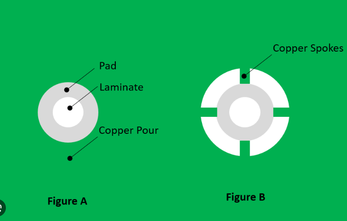
Thermal relief pads are specialized copper pads that connect a component’s thermal pad to the PCB’s ground or power plane through a series of narrow traces, often referred to as “spokes.”
These spokes create a controlled thermal path that allows heat to dissipate while also providing electrical connectivity. One of the primary advantages of thermal relief pads is their ability to facilitate the soldering process. The narrow traces reduce the amount of heat required to melt the solder, thereby minimizing the risk of thermal damage to the component or the PCB itself. This is particularly beneficial during the reflow soldering process, where precise temperature control is crucial.
In contrast, direct thermal connections involve a solid copper connection between the component’s thermal pad and the PCB’s ground or power plane.
This method provides a more efficient thermal path, allowing for superior heat dissipation. Direct thermal connections are often used in high-power applications where effective thermal management is paramount. However, this approach can pose challenges during the soldering process. The large copper area can act as a heat sink, requiring higher temperatures and longer soldering times to achieve a reliable joint. This can increase the risk of thermal stress and potential damage to both the component and the PCB.
When comparing thermal relief pads and direct thermal connections, it is important to consider the specific requirements of the application.
For low to moderate power applications, thermal relief pads often provide a balanced solution that ensures adequate heat dissipation while simplifying the soldering process. The controlled thermal path created by the spokes helps to prevent overheating and ensures a reliable electrical connection. Additionally, thermal relief pads can reduce the risk of solder bridging, which can occur when excess solder flows between adjacent pads, causing short circuits.
On the other hand, direct thermal connections are more suitable for high-power applications where efficient heat dissipation is critical.
The solid copper connection provides a low thermal resistance path, allowing heat to be quickly transferred away from the component. This can help to prevent thermal runaway and ensure the long-term reliability of the device. However, designers must carefully consider the soldering process and may need to implement additional measures, such as preheating or using specialized soldering techniques, to mitigate the challenges associated with direct thermal connections.
In conclusion, the choice between thermal relief pads and direct thermal connections in PCB design depends on a variety of factors, including the power requirements of the application, the thermal management needs, and the manufacturability considerations. Thermal relief pads offer a balanced approach that simplifies the soldering process and provides adequate heat dissipation for low to moderate power applications. In contrast, direct thermal connections provide superior thermal performance for high-power applications but require careful attention to the soldering process to avoid potential issues. By understanding the advantages and limitations of each method, designers can make informed decisions that optimize the performance and reliability of their PCBs.