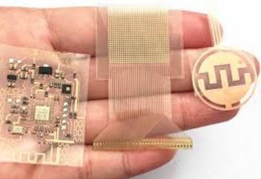
Thinnest flex pcb
Advantages Of Using Thinnest Flex PCBs In Modern Electronics
The advent of the thinnest flexible printed circuit boards (PCBs) has revolutionized the landscape of modern electronics, offering a myriad of advantages that cater to the ever-evolving demands of contemporary technology.
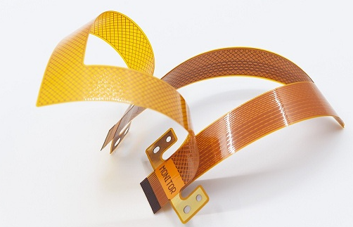
One of the most significant benefits of these ultra-thin flex PCBs is their unparalleled flexibility,
which allows for innovative design possibilities that were previously unattainable with traditional rigid PCBs. This flexibility enables the creation of compact, lightweight devices that can be bent, folded, or twisted without compromising their functionality, making them ideal for applications in wearable technology, medical devices, and other compact electronic gadgets.
Moreover, the reduced thickness of these flex PCBs contributes to a substantial decrease in the overall weight of electronic devices.
This weight reduction is particularly advantageous in the aerospace and automotive industries, where every gram counts towards improving fuel efficiency and performance. Additionally, the thin profile of these PCBs allows for more efficient use of space within electronic devices, facilitating the integration of more components and features without increasing the device’s size. This space-saving attribute is crucial in the development of next-generation smartphones, tablets, and other portable electronics, where consumers demand ever-more powerful and feature-rich devices in increasingly smaller form factors.
Another notable advantage of the thinnest flex PCBs is their enhanced reliability and durability.
The inherent flexibility of these PCBs allows them to absorb and dissipate mechanical stress more effectively than their rigid counterparts, reducing the risk of damage due to bending, vibration, or thermal expansion. This resilience is particularly beneficial in applications where electronic devices are subjected to harsh environmental conditions or frequent mechanical stress, such as in industrial automation, military equipment, and automotive electronics. Furthermore, the use of advanced materials and manufacturing techniques in the production of these flex PCBs ensures high-quality performance and longevity, even in demanding applications.
In addition to their mechanical advantages, the thinnest flex PCBs also offer significant electrical benefits.
The reduced thickness of these PCBs results in shorter signal paths, which can lead to improved signal integrity and faster transmission speeds. This is particularly important in high-frequency applications, such as telecommunications and data processing, where maintaining signal quality and minimizing latency are critical. Moreover, the ability to design complex, multi-layer flex PCBs allows for greater circuit density and functionality, enabling the development of more sophisticated and capable electronic systems.
The environmental impact of electronic devices is an increasingly important consideration in today’s world, and the thinnest flex PCBs offer several eco-friendly advantages.
The reduced material usage in these PCBs not only decreases the overall weight and size of electronic devices but also minimizes the consumption of raw materials and energy during the manufacturing process. Additionally, the flexibility and durability of these PCBs can extend the lifespan of electronic devices, reducing the frequency of replacements and the associated electronic waste. This sustainability aspect is particularly appealing to environmentally conscious consumers and companies striving to reduce their ecological footprint.
In conclusion, the thinnest flexible PCBs present a host of advantages that make them an indispensable component in modern electronics. Their unparalleled flexibility, space-saving attributes, enhanced reliability, and electrical benefits, coupled with their eco-friendly characteristics, position them as a key enabler of innovation in various industries. As technology continues to advance, the adoption of these ultra-thin flex PCBs is poised to grow, driving the development of increasingly sophisticated, compact, and sustainable electronic devices.
Manufacturing Techniques For Thinnest Flex PCBs
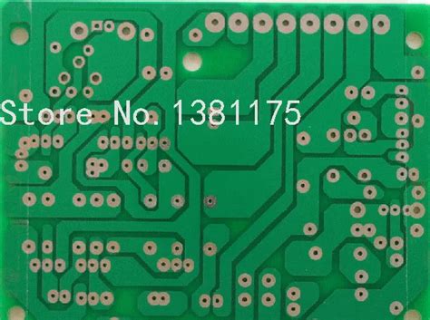
The manufacturing techniques for the thinnest flexible printed circuit boards (PCBs) have evolved significantly, driven by the demand for miniaturization and enhanced performance in modern electronic devices. These advancements are crucial for applications in industries such as consumer electronics, medical devices, and aerospace, where space constraints and flexibility are paramount. To achieve the thinnest flex PCBs, manufacturers employ a combination of innovative materials, precise fabrication processes, and meticulous quality control measures.
One of the primary considerations in producing ultra-thin flex PCBs is the selection of appropriate materials.
Polyimide films are commonly used due to their excellent thermal stability, mechanical strength, and flexibility. These films can be as thin as 12.5 micrometers, providing a robust yet pliable substrate for the circuit. Additionally, the use of advanced copper foils, which can be as thin as 9 micrometers, is essential for creating the conductive traces. The combination of these materials ensures that the final product is both durable and capable of withstanding the rigors of various applications.
Transitioning from material selection to the fabrication process, photolithography plays a pivotal role in defining the circuit patterns on the flex PCB.
This technique involves coating the polyimide substrate with a photoresist, exposing it to ultraviolet light through a mask, and then developing the exposed areas to reveal the desired circuit pattern. The precision of photolithography allows for the creation of extremely fine features, which is critical for maintaining the integrity of the circuit in such a thin form factor.
Following photolithography, the next step is the etching process, where unwanted copper is removed to leave behind the intricate circuit traces.
Chemical etching is commonly used, as it provides the necessary accuracy and control. However, to further enhance the precision, manufacturers may employ laser etching techniques. Laser etching offers the advantage of being able to create even finer details and more complex geometries, which are often required in advanced electronic applications.
Once the circuit pattern is established, the next phase involves the application of protective layers and surface finishes.
These layers are crucial for ensuring the reliability and longevity of the flex PCB. Solder mask, for instance, is applied to protect the copper traces from oxidation and to prevent short circuits during soldering. Additionally, surface finishes such as immersion gold or organic solderability preservatives (OSP) are used to enhance solderability and protect the exposed copper pads.
Quality control is an integral part of the manufacturing process for thinnest flex PCBs.
Given the delicate nature of these circuits, rigorous inspection and testing are necessary to identify and rectify any defects. Automated optical inspection (AOI) systems are employed to detect issues such as misalignments, open circuits, and short circuits. Furthermore, electrical testing ensures that the circuit performs as intended under various conditions.
In conclusion, the manufacturing techniques for the thinnest flex PCBs involve a meticulous blend of material selection, precise fabrication processes, and stringent quality control measures. The use of advanced materials like polyimide films and ultra-thin copper foils, combined with photolithography and laser etching, enables the creation of highly reliable and flexible circuits. As technology continues to advance, these techniques will undoubtedly evolve, paving the way for even thinner and more sophisticated flex PCBs that meet the ever-growing demands of modern electronic applications.
Applications Of Thinnest Flex PCBs In Wearable Technology
The advent of the thinnest flexible printed circuit boards (PCBs) has revolutionized the landscape of wearable technology, offering unprecedented opportunities for innovation and functionality.
These ultra-thin, highly adaptable circuits are integral to the development of next-generation wearables, providing a foundation for devices that are not only more efficient but also more comfortable and versatile for users. As we delve into the applications of the thinnest flex PCBs in wearable technology, it becomes evident that their impact is both profound and far-reaching.
One of the primary applications of the thinnest flex PCBs in wearable technology is in the realm of health monitoring devices.
These devices, which include fitness trackers, heart rate monitors, and even advanced medical sensors, benefit immensely from the flexibility and reduced bulk of these PCBs. The thinness of the circuits allows for a more seamless integration into fabrics and other materials, making the devices less intrusive and more comfortable for continuous wear. Consequently, users are more likely to wear these devices consistently, leading to more accurate and comprehensive health data collection.
In addition to health monitoring, the thinnest flex PCBs are also pivotal in the development of smart clothing.
Smart textiles, which incorporate electronic components directly into the fabric, rely on the flexibility and durability of these PCBs to maintain functionality without compromising comfort. For instance, athletes can wear smart clothing that monitors their performance metrics, such as heart rate, muscle activity, and body temperature, in real-time. The data collected can then be analyzed to optimize training regimens and improve overall performance. The thinness of the PCBs ensures that the clothing remains lightweight and breathable, essential qualities for athletic wear.
Moreover, the integration of the thinnest flex PCBs extends to the realm of augmented reality (AR) and virtual reality (VR) wearables.
AR and VR headsets, gloves, and other accessories require intricate circuitry to function effectively. The use of ultra-thin flex PCBs allows these devices to be more ergonomic and less cumbersome, enhancing the user experience. For example, VR gloves equipped with these PCBs can provide more precise motion tracking and haptic feedback, making virtual interactions more immersive and realistic. The reduced weight and increased flexibility also contribute to longer usage periods without discomfort.
Furthermore, the thinnest flex PCBs are instrumental in the advancement of wearable communication devices.
Smartwatches and other wearable gadgets that facilitate communication benefit from the compact and flexible nature of these circuits. The reduced size allows for more sophisticated features to be packed into smaller devices, enhancing their functionality while maintaining a sleek design. This is particularly important as consumers demand more from their wearable devices, expecting them to perform a wide range of tasks from messaging and calling to health monitoring and navigation.
In conclusion, the applications of the thinnest flex PCBs in wearable technology are vast and varied, driving significant advancements across multiple domains. From health monitoring and smart clothing to AR/VR devices and wearable communication gadgets, these ultra-thin circuits are at the heart of innovation. Their ability to provide flexibility, durability, and reduced bulk makes them indispensable in the quest to create more efficient, comfortable, and versatile wearable technology. As research and development in this field continue to progress, we can anticipate even more groundbreaking applications and improvements in the wearables we rely on daily.
Challenges And Solutions In Designing Thinnest Flex PCBs
Designing the thinnest flexible printed circuit boards (PCBs) presents a unique set of challenges and requires innovative solutions to overcome them. As the demand for smaller, lighter, and more versatile electronic devices continues to grow, engineers and designers are pushed to the limits of current technology to create PCBs that meet these stringent requirements.
One of the primary challenges in designing the thinnest flex PCBs is maintaining structural integrity while reducing thickness.
Traditional PCBs rely on multiple layers of materials, including copper and insulating substrates, to provide the necessary electrical pathways and mechanical support. However, as the thickness of these layers is reduced, the risk of mechanical failure increases. To address this issue, advanced materials such as polyimide and liquid crystal polymer (LCP) are often used due to their excellent mechanical properties and thermal stability.
Another significant challenge is ensuring reliable electrical performance in ultra-thin flex PCBs.
As the thickness of the conductive traces is reduced, the resistance of these traces increases, which can lead to signal integrity issues and power losses. To mitigate these problems, designers must carefully optimize the trace width and spacing, as well as employ advanced fabrication techniques such as laser direct structuring (LDS) and additive manufacturing. These methods allow for precise control over the deposition of conductive materials, resulting in higher-quality traces with improved electrical performance.
Thermal management is also a critical concern in the design of thinnest flex PCBs.
As electronic devices become more compact, the heat generated by the components must be efficiently dissipated to prevent overheating and ensure reliable operation. Traditional cooling methods, such as heat sinks and fans, are often impractical for ultra-thin flex PCBs due to their size and weight constraints. Instead, designers must rely on innovative thermal management solutions, such as the use of thermally conductive materials and the integration of microfluidic cooling channels within the PCB itself. These approaches help to effectively dissipate heat while maintaining the overall thinness of the PCB.
In addition to these technical challenges, the manufacturing process for thinnest flex PCBs also presents several difficulties.
The delicate nature of ultra-thin materials makes them more susceptible to damage during handling and processing. To minimize the risk of defects, manufacturers must employ specialized equipment and techniques, such as roll-to-roll processing and automated optical inspection (AOI) systems. These methods help to ensure consistent quality and reduce the likelihood of defects that could compromise the performance of the final product.
Despite these challenges, the development of thinnest flex PCBs offers numerous benefits that make them an attractive option for a wide range of applications.
Their lightweight and flexible nature make them ideal for use in wearable electronics, medical devices, and other applications where traditional rigid PCBs would be impractical. Furthermore, the ability to create ultra-thin PCBs opens up new possibilities for the design of compact and innovative electronic devices, enabling the development of next-generation technologies.
In conclusion, the design and manufacture of the thinnest flex PCBs involve overcoming a variety of challenges related to structural integrity, electrical performance, thermal management, and manufacturing processes. By leveraging advanced materials, fabrication techniques, and innovative thermal management solutions, engineers and designers can create ultra-thin flex PCBs that meet the demanding requirements of modern electronic devices. As technology continues to advance, the development of even thinner and more versatile flex PCBs will undoubtedly play a crucial role in shaping the future of electronics