Times are changing, but the golden rules of PCB design remain the same.
The following content of this article introduces the ten most effective design rules that electronic design engineers should keep in mind and practice when using design software for PCB layout design and commercial manufacturing. Engineers do not need to implement these laws in chronological order or relative importance; simply following them all can dramatically change product design.
Rule 1: Choose the right grid
Set and always use a grid spacing that matches the most components. While multi-grid may seem like a powerful solution, if engineers think a little more early in PCB layout design, they can avoid spacing difficulties and maximize board utilization. Because many devices come in multiple package sizes, engineers should use the product that best suits their design.
In addition, polygons are critical to circuit board copper routing. Multi-grid circuit boards generally produce polygon fill deviations when polygonal copper routing is performed. Although not as standard as a single grid-based one, it can provide longer than required board life. .
Rule 2: Keep the path the shortest and most direct
This may sound simple and mundane, but it should be kept in mind at every stage, even if it means changing the board layout to optimize trace lengths. This is especially true for analog and high-speed digital circuits where system performance is always limited in part by impedance and parasitic effects.
Rule 3: Use the power layer as much as possible to manage the distribution of power lines and ground lines
Coppering the power plane is a faster and easier option for most PCB design software. By having a large number of wires with a common connection, the most efficient flow of current with minimal impedance or voltage drop is ensured while providing an adequate return path to ground.
If possible, you can also run multiple power supply lines in the same area of the circuit board to confirm whether the ground layer covers most of a certain layer of the PCB. This will facilitate the interaction between lines running on adjacent layers.
Rule 4: Group related components together with the required test points
For example: Placing the discrete components required for the OpAmp op amp closer to the device so that the bypass capacitors and resistors can co-locate with them helps optimize the trace lengths mentioned in Rule 2 while also enabling test and fault detection. becomes easier.
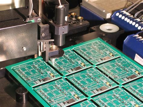
Rule 5: Repeat the required circuit board on another larger circuit board multiple times for PCB imposition
Choosing the size that best fits the equipment used by the manufacturer can help reduce prototyping and manufacturing costs.
Start by laying out the board on the panel, contact the board manufacturer to get their preferred size specifications for each panel, then modify your design specifications and try to make multiple iterations of your design within those panel sizes.
Rule 6: Integrate component values.
As a designer, you will choose discrete components with higher or lower component values but the same performance. By consolidating within a smaller range of standard values, the bill of materials can be simplified and costs can potentially be reduced. If you have a range of PCB products based on preferred device values, it will also help you make the right inventory management decisions in the longer term.
Rule 7: Perform as many design rule checks (DRCs) as possible.
Although it only takes a short time to run the DRC function on PCB software, in more complex design environments, you can save a lot of time as long as you perform checks throughout the design process. This is a good habit worth maintaining. Every routing decision is critical, and performing DRC will remind you of the most important routing decisions at any time.
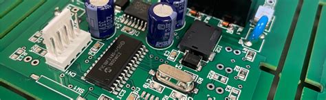
Rule 8: Use screen printing flexibly.
Screen printing can be used to label a variety of useful information for future use by circuit board manufacturers, service or test engineers, installers, or equipment tuners. Not only are functions and test points clearly labeled, but component and connector orientations are indicated wherever possible, even if these notes are printed on the underside of the components used on the board (after the board is assembled).
The full application of screen printing technology on the upper and lower surfaces of the circuit board can reduce duplication of work and streamline the production process.
Rule 9: Decoupling capacitors must be selected
Don’t try to optimize your design by avoiding decoupled power lines and relying on the extreme values in the component data sheet. Capacitors are cheap and durable, and you can spend as much time as possible putting them together while following Rule 6 and using standard value ranges to keep your inventory tidy.
Rule 10: Generate PCB manufacturing parameters and verify them before submitting for production
While most circuit board manufacturers will be happy to download it and verify it for you, it’s best to export the Gerber file yourself and use a free viewer to check that it’s as expected to avoid misunderstandings.
By checking it yourself, you may even catch some inadvertent mistakes and avoid costly production to the wrong parameters.
As circuit designs become more widely shared and internal teams increasingly rely on reference designs, basic rules like the above will continue to be a feature of printed circuit board design, and we believe they are important for PCB design. With these basic rules in mind, developers have the flexibility to increase the value of their products and get the most from the boards they build.
Even if you are new to circuit board design, remembering these basic rules will speed up the learning process and increase your confidence.
For embedded technology learning, contact Teacher Song Penguin number: 3524-6590-88 Tel/WX: 173–1795–1908
The following courses are available for free trial in C language, electronics, PCB, STM32, Linux, FPGA, JAVA, Android, etc.


