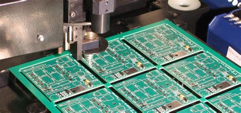
Top 10 tips for high speed pcb design
Essential Layout Tips For High Speed PCB Design
When designing high-speed printed circuit boards (PCBs), it is crucial to adhere to certain layout principles to ensure optimal performance and reliability.
One of the most essential tips is to maintain a clear and concise signal path.
This involves minimizing the length of traces, which helps to reduce signal degradation and electromagnetic interference (EMI). By keeping traces as short as possible, you can also minimize the potential for signal reflections, which can cause data corruption and timing issues.
Another important consideration is the use of proper grounding techniques.
A solid ground plane is essential for high-speed PCB design, as it provides a low-impedance path for return currents and helps to reduce noise. Ensuring that the ground plane is continuous and unbroken can significantly improve the overall performance of the PCB. Additionally, placing decoupling capacitors close to the power pins of integrated circuits (ICs) can help to filter out high-frequency noise and provide a stable power supply.
Signal integrity is another critical aspect of high-speed PCB design.
To maintain signal integrity, it is important to control the impedance of traces. This can be achieved by carefully selecting the trace width and spacing, as well as the dielectric material used in the PCB. Impedance matching is particularly important for differential pairs, which are commonly used in high-speed designs to reduce noise and crosstalk. Ensuring that differential pairs are routed together with consistent spacing and length can help to maintain signal integrity and improve overall performance.
In addition to controlling impedance, it is also important to manage crosstalk between adjacent traces.
Crosstalk can be minimized by increasing the spacing between traces and using ground planes to shield sensitive signals. Additionally, routing high-speed signals on internal layers, sandwiched between ground planes, can help to reduce crosstalk and improve signal integrity.
Thermal management is another essential aspect of high-speed PCB design. High-speed components can generate significant amounts of heat, which can affect the performance and reliability of the PCB. To manage heat effectively, it is important to use thermal vias and heat sinks to dissipate heat away from critical components. Additionally, ensuring that there is adequate airflow around the PCB can help to keep temperatures within acceptable limits.
Proper component placement is also crucial for high-speed PCB design.
Placing components in close proximity to each other can help to minimize trace lengths and reduce signal degradation. Additionally, grouping components with similar functions together can help to simplify routing and improve overall performance. It is also important to consider the placement of connectors and other interface components, as these can introduce noise and affect signal integrity.
Another key tip for high-speed PCB design is to use controlled impedance traces for high-speed signals. Controlled impedance traces help to ensure that signals are transmitted with minimal distortion and signal loss. This can be achieved by carefully designing the trace geometry and selecting the appropriate materials for the PCB.
Finally, it is important to perform thorough testing and validation of the PCB design.
This includes using simulation tools to analyze signal integrity, power integrity, and thermal performance. Additionally, performing physical testing of prototypes can help to identify and address any issues before the final production run.
In conclusion, high-speed PCB design requires careful attention to detail and adherence to best practices. By following these essential layout tips, you can ensure that your high-speed PCB designs are reliable, efficient, and capable of meeting the demands of modern electronic systems.
Top 10 Signal Integrity Tips For High Speed PCB Design
Designing high-speed printed circuit boards (PCBs) requires meticulous attention to signal integrity to ensure optimal performance and reliability. Signal integrity issues can lead to data corruption, electromagnetic interference, and overall system failure. Therefore, adhering to best practices is crucial. Here are the top 10 signal integrity tips for high-speed PCB design.
Firstly, it is essential to maintain controlled impedance throughout the PCB.
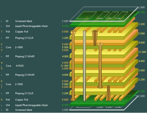
Controlled impedance ensures that the signal transmission lines have consistent electrical characteristics, which is vital for high-speed signals. This can be achieved by carefully designing the trace width, spacing, and the dielectric material used in the PCB stack-up.
Secondly, minimizing crosstalk is critical. Crosstalk occurs when a signal in one trace induces an unwanted signal in an adjacent trace.
To mitigate this, designers should maintain adequate spacing between high-speed traces and use ground planes to provide a return path for the signals. Additionally, differential pairs should be routed together to cancel out any induced noise.
Another important tip is to use proper termination techniques.
Termination resistors can help match the impedance of the transmission line to the load, thereby reducing reflections and signal degradation. Series and parallel termination are common methods, and the choice depends on the specific requirements of the design.
Furthermore, it is advisable to keep signal paths as short as possible.
Long traces can act as antennas, picking up noise and causing signal degradation. By minimizing the length of high-speed signal paths, designers can reduce the potential for signal integrity issues.
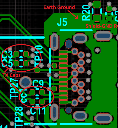
In addition, careful consideration should be given to the placement of decoupling capacitors. These capacitors help to filter out noise and provide a stable power supply to the components. Placing them close to the power pins of integrated circuits and using multiple capacitors with different values can improve the overall performance of the PCB.
Ground planes play a significant role in maintaining signal integrity.
A solid ground plane provides a low-impedance return path for signals, reducing noise and electromagnetic interference. It is important to avoid splitting ground planes, as this can create impedance discontinuities and degrade signal quality.
Moreover, differential signaling is a preferred method for high-speed designs.
Differential pairs consist of two complementary signals that are routed together. This technique helps to cancel out common-mode noise and improves signal integrity. Ensuring that the differential pairs are tightly coupled and have equal lengths is crucial for maintaining signal quality.
Another key aspect is the use of vias.
Vias are used to connect different layers of the PCB, but they can introduce impedance discontinuities and signal reflections. To minimize these effects, designers should use as few vias as possible and ensure that the via structures are properly designed.
Additionally, it is important to consider the impact of the PCB layout on signal integrity.
Proper layer stacking, trace routing, and component placement can significantly affect the performance of high-speed signals. Using simulation tools to analyze the PCB layout can help identify potential issues and optimize the design.
Lastly, thorough testing and validation are essential. Once the PCB is designed and fabricated, it is crucial to perform signal integrity testing to ensure that the design meets the required specifications. Tools such as oscilloscopes, network analyzers, and time-domain reflectometers can be used to measure signal quality and identify any issues that need to be addressed.
In conclusion, maintaining signal integrity in high-speed PCB design requires careful consideration of various factors, including controlled impedance, crosstalk minimization, proper termination, short signal paths, decoupling capacitor placement, ground planes, differential signaling, via usage, PCB layout, and thorough testing. By following these top 10 tips, designers can ensure that their high-speed PCBs perform reliably and efficiently.

Power Distribution Tips For High Speed PCB Design
In the realm of high-speed PCB design, power distribution is a critical aspect that can significantly influence the performance and reliability of the final product. Ensuring efficient power distribution requires meticulous planning and execution. Here are ten essential tips to help you achieve optimal power distribution in your high-speed PCB designs.
Firstly, it is imperative to use a solid ground plane.
A continuous ground plane reduces the impedance of the return path, thereby minimizing noise and ensuring signal integrity. This practice also helps in reducing electromagnetic interference (EMI), which is crucial for maintaining the performance of high-speed circuits.
Secondly, decoupling capacitors play a vital role in stabilizing the power supply.
Placing these capacitors close to the power pins of integrated circuits (ICs) helps in filtering out high-frequency noise. It is advisable to use a combination of capacitors with different values to cover a broad range of frequencies, ensuring a stable power supply across the entire spectrum.
Another important tip is to use power planes instead of power traces.
Power planes provide a low-impedance path for the current, which is essential for high-speed designs. They also help in distributing power evenly across the PCB, reducing voltage drops and ensuring that all components receive a stable supply.
In addition, it is crucial to pay attention to the layout of power and ground planes.
Ensuring that these planes are as close as possible to each other helps in reducing the loop area, which in turn minimizes inductance and EMI. This practice is particularly important in high-speed designs where even small amounts of noise can have a significant impact on performance.
Moreover, the use of via stitching can enhance the performance of power distribution networks.
Via stitching involves placing multiple vias around the power and ground planes to create a low-impedance path. This technique helps in reducing the inductance and resistance of the power distribution network, ensuring a stable power supply to all components.
Thermal management is another critical aspect of power distribution in high-speed PCB design.
High-speed circuits tend to generate a significant amount of heat, which can affect the performance and reliability of the components. Using thermal vias and heat sinks can help in dissipating heat effectively, ensuring that the components operate within their specified temperature range.
Furthermore, it is essential to consider the power requirements of each component during the design phase.
Understanding the current consumption and voltage requirements of each component helps in designing an efficient power distribution network. This practice also helps in selecting the appropriate power supply and ensuring that it can meet the demands of the entire system.
Additionally, it is advisable to use ferrite beads in the power distribution network.
Ferrite beads act as low-pass filters, blocking high-frequency noise while allowing DC and low-frequency signals to pass through. Placing ferrite beads at strategic locations can help in reducing noise and ensuring a stable power supply.
Another important consideration is the use of power integrity analysis tools.
These tools help in simulating the power distribution network and identifying potential issues such as voltage drops and noise. Using these tools during the design phase can help in optimizing the power distribution network and ensuring that it meets the performance requirements.
Lastly, it is crucial to follow best practices for PCB layout and routing.
Ensuring that power and ground traces are wide enough to handle the current, avoiding sharp corners, and maintaining proper spacing between traces can help in reducing noise and ensuring a stable power supply.
In conclusion, efficient power distribution is essential for the performance and reliability of high-speed PCB designs. By following these ten tips, you can ensure that your power distribution network is optimized for high-speed operation, resulting in a stable and reliable final product.

Top 10 Routing Strategies For High Speed PCB Design
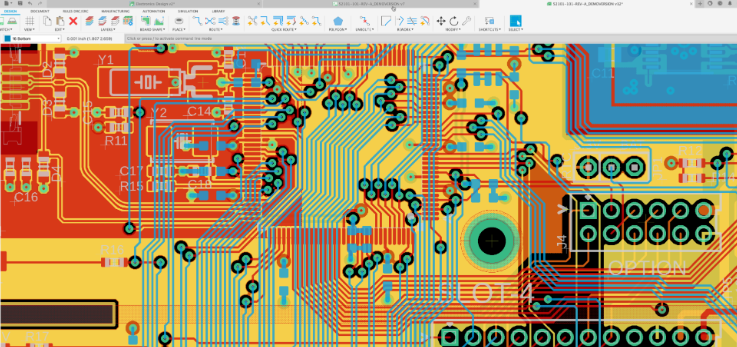
When designing high-speed printed circuit boards (PCBs), effective routing strategies are crucial to ensure signal integrity, minimize electromagnetic interference (EMI), and achieve optimal performance. The first strategy to consider is maintaining controlled impedance. This involves designing traces with specific widths and spacing to match the impedance requirements of high-speed signals. Controlled impedance helps prevent signal reflections and ensures consistent signal transmission.
Next, it is essential to use differential pairs for high-speed signals.
Differential pairs consist of two traces that carry equal and opposite signals. This technique reduces noise and crosstalk, as the electromagnetic fields generated by the signals cancel each other out. Properly matched differential pairs also improve signal integrity and reduce EMI.
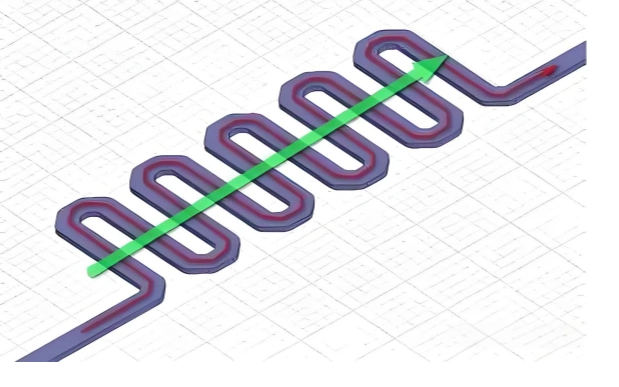
Another important strategy is to minimize the length of high-speed signal traces.
Shorter traces reduce the potential for signal degradation and timing issues. When long traces are unavoidable, it is advisable to use serpentine routing to match the lengths of critical signal paths, ensuring that signals arrive at their destinations simultaneously.
Ground planes play a significant role in high-speed PCB design.
A continuous ground plane provides a low-impedance return path for signals, reducing noise and EMI. It is crucial to avoid splitting ground planes, as this can create impedance discontinuities and increase the risk of signal integrity issues. Additionally, placing high-speed signal traces over a solid ground plane helps maintain controlled impedance.
Via management is another critical aspect of high-speed PCB routing.
Vias introduce inductance and capacitance, which can affect signal integrity. To mitigate these effects, it is advisable to minimize the number of vias in high-speed signal paths. When vias are necessary, using blind or buried vias can help reduce their impact on signal performance.
Crosstalk is a common issue in high-speed PCB design, and it can be mitigated by maintaining adequate spacing between signal traces.
Increasing the distance between traces reduces the potential for electromagnetic coupling, which can cause unwanted interference. Additionally, routing high-speed signals on different layers or using ground traces between signal traces can further reduce crosstalk.
Power integrity is also crucial in high-speed PCB design.
Ensuring a stable power supply involves using decoupling capacitors to filter out noise and provide a low-impedance path for high-frequency currents. Placing these capacitors close to the power pins of integrated circuits (ICs) helps maintain power integrity and reduces the risk of signal degradation.
Signal return paths must be carefully managed to avoid creating loops that can act as antennas and radiate EMI. Ensuring that return paths are as short and direct as possible helps minimize loop areas and reduces the potential for EMI. Additionally, using ground planes and stitching vias can help provide continuous return paths for high-speed signals.
Another effective strategy is to use proper termination techniques to match the impedance of signal traces and prevent reflections.
Series and parallel termination resistors can be used to match the impedance of the source and load, ensuring that signals are transmitted without significant reflections.
Finally, it is essential to perform thorough signal integrity analysis during the design process. Simulation tools can help identify potential issues and optimize routing strategies before the PCB is manufactured. By analyzing signal integrity, designers can make informed decisions and implement best practices to ensure the performance and reliability of high-speed PCBs.
In conclusion, high-speed PCB design requires careful consideration of various routing strategies to ensure signal integrity, minimize EMI, and achieve optimal performance. By implementing these top 10 routing strategies, designers can create high-speed PCBs that meet the demanding requirements of modern electronic system