Top 6 PCB Design Guidelines to Know for a Functional and Reliable PCB
When starting a new design, most of the time is spent on circuit design and component selection, which often leads to less careful consideration during the PCB layout and routing phase due to lack of experience.
Failure to provide sufficient time and effort for the design during the PCB layout and routing phase can lead to problems during the manufacturing phase or defects in functionality when the design is translated from the digital realm to physical reality.
So what is the key to designing a circuit board that is both realistic and reliable on paper and in physical form? Let’s explore the top 6 PCB design guidelines to know when designing a manufacturable, functional and reliable PCB.
1.Fine-tune your component placement
The component placement phase of the PCB layout process is both a science and an art, requiring strategic consideration of the major components available on the board. While this process can be challenging, the way you place the electronic components will determine how easy your board is to manufacture and how well it meets your original design requirements. While there is a general order for component placement, such as placing connectors, PCB mounting devices, power circuits, precision circuits, critical circuits, etc. in order, there are also specific guidelines to keep in mind, including:
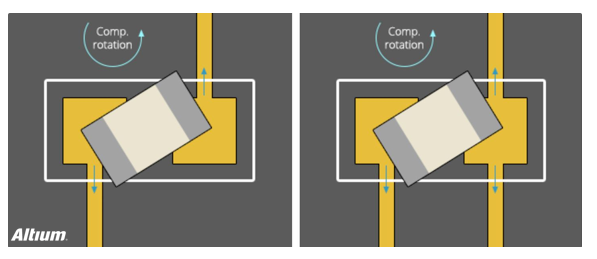
Orientation – Make sure to position similar components in the same direction, which will help achieve an efficient and error-free soldering process.
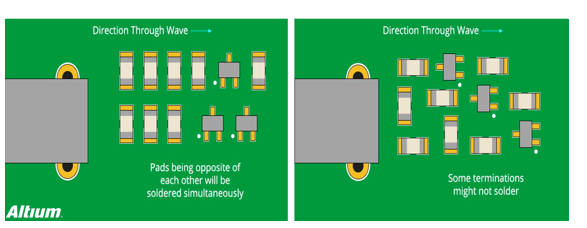
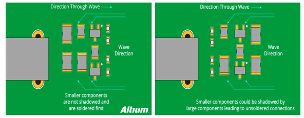
Layout – Avoid placing smaller components behind larger components, which may cause problems with the soldering of large components.
Organization – It is recommended to place all surface mount (SMT) components on the same side of the board and all through-hole (TH) components on the top of the board to minimize assembly steps.
One last PCB design guideline to note – when using mixed technology components (through-hole and surface mount components), the manufacturer may require additional processes to assemble the board, which will increase your overall cost.
Good chip component orientation (left) and bad chip component orientation (right)
Good component placement (left) and bad component placement (right)
2.Proper placement of power, ground, and signal traces
After placing the components, you can next place the power, ground, and signal traces to ensure that your signals have a clean and trouble-free path to pass. At this stage of the layout process, keep in mind some of the following guidelines:
1) Positioning the power and ground plane layers
It is always recommended to place the power and ground plane layers inside the board while keeping them symmetrical and centered. This helps prevent your board from bowing, which also relates to whether your components are properly positioned. For powering ICs, it is recommended to use a common channel for each power supply, ensure a strong and stable routing width, and avoid daisy-chain power connections between components.
2) Signal line routing connection
Next, connect the signal lines according to the design in the schematic diagram. It is recommended to always take the shortest possible path and direct path routing between components. If your components need to be fixed in the horizontal direction without deviation, it is recommended to basically route horizontally where the components of the circuit board are connected, and then route vertically after the connection. In this way, as the solder migrates during welding, the components will be fixed in the horizontal direction. As shown in the upper half of the figure below. The signal routing method in the lower half of the figure below may cause the component to deflect as the solder flows during welding.

Recommended routing (arrows indicate solder flow direction)
Not recommended routing (arrows indicate solder flow direction)
3) Define network width
Your design may require different networks that will carry various currents, which will determine the required network width. With this basic requirement in mind, it is recommended to provide 0.010” (10mil) width for low-current analog and digital signals. When your line current exceeds 0.3 amps, it should be widened. Here is a free line width calculator to make this conversion process simple.
3.Effective isolation
You may have experienced how large voltage and current spikes in the power supply circuit can interfere with your low-voltage current control circuit. To minimize such interference issues, follow these guidelines:
Isolation – Make sure to keep the power and control grounds separate for each power supply. If you must connect them together in the PCB, make sure it is as close to the end of the power path as possible.
Layout – If you have placed a ground plane on the middle layer, make sure to place a low impedance path to reduce the risk of any power circuit interference and help protect your control signals. The same guidelines can be followed to keep your digital and analog separate.
Coupling – To reduce capacitive coupling due to placing a large ground plane and the traces above and below it, try to cross the analog ground only with analog signal lines.
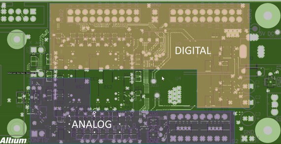
Component Isolation Example (Digital and Analog)
4.Solve Heat Issues
Have you ever experienced a degradation of circuit performance or even board damage due to heat issues? Many designers have encountered many problems due to not considering heat dissipation. Here are some guidelines to keep in mind to help solve thermal issues:
1) Identify troublesome components
The first step is to start thinking about which components will dissipate the most heat on the board. This can be done by first finding the “thermal resistance” rating in the component’s datasheet, and then following the recommended guidelines to divert the generated heat. Of course, heat sinks and cooling fans can be added to keep component temperatures down, and also remember to keep critical components away from any high heat sources.
2) Add hot air pads
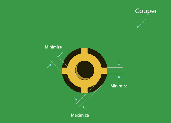
Adding hot air pads is very useful for producing manufacturable boards, and they are essential for wave soldering applications on high copper content components and multi-layer boards. Because it is difficult to maintain process temperatures, it is always recommended to use hot air pads on through-hole components to make the soldering process as simple as possible by slowing the heat dissipation rate at the component pins. As a general guideline, always use hot air pads for any through-holes or vias that connect to the ground plane or power plane. In addition to hot air pads, you can also add teardrops where the pads connect to the wires to provide additional copper foil/metal support. This will help reduce mechanical and thermal stress.

Typical hot air soldering pad connection method
5.Popular knowledge of hot air soldering pad
Many engineers in charge of process or SMT technology in factories often encounter problems such as empty soldering, de-wetting or cold soldering on circuit board components. No matter how the process conditions are changed or the reflow oven temperature is adjusted, there is a certain rate of non-wetting. What is going on? Apart from the problem of component and circuit board oxidation, the root cause is that a large part of this type of poor soldering actually comes from the lack of layout design of the circuit board. The most common problem is that some of the solder pins of the component are connected to a large area of copper foil, causing these component solder pins to have poor soldering after reflow soldering. Some hand-soldered components may also cause de-wetting or package soldering problems due to similar situations. Some components are even damaged due to overheating. Generally, when designing PCB circuits, it is often necessary to lay a large area of copper foil as power supply (Vcc, Vdd or Vss) and ground (GND, Ground). These large areas of copper foil are generally directly connected to some control circuits (IC) and pins of electronic components. Unfortunately, if we want to heat these large areas of copper foil to the temperature of melting tin, it usually takes more time than independent solder pads (that is, the heating will be slower), and the heat dissipation is also faster. When one end of such a large area of copper foil wiring is connected to small components such as small resistors and small capacitors, and the other end is not, it is easy to cause welding problems due to inconsistent melting and solidification time; if the temperature curve of reflow soldering is not adjusted well and the preheating time is insufficient, the solder feet of these components connected to the large piece of copper foil are easy to cause cold soldering problems because they cannot reach the melting temperature. When hand soldering, these component solder feet connected to the large piece of copper foil will not be able to complete the soldering within the specified time due to too fast heat dissipation. The most common defective phenomenon is solder wrapping and cold soldering, where the solder is only soldered on the solder pins of the component but not connected to the pads of the circuit board. From the appearance, the entire solder joint will form a ball shape; even worse, the operator keeps raising the temperature of the soldering iron in order to solder the solder pins to the circuit board, or heats it for too long, causing the component to exceed the heat resistance temperature and be damaged without knowing it. As shown in the figure below.
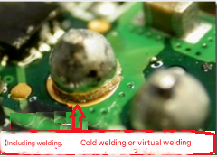
Solder wrapping, cold soldering or cold soldering Since we know the problem point, we can have a solution. Generally, we will require the so-called Thermal Relief pad design to solve this type of welding problem caused by large pieces of copper foil connecting the solder pins of components. As shown in the figure below, the wiring on the left does not use the hot air solder pad, while the wiring on the right has been connected using the hot air solder pad. You can see that the contact area between the solder pad and the large copper foil is only a few small lines, which can greatly limit the loss of temperature on the solder pad and achieve a better soldering effect.
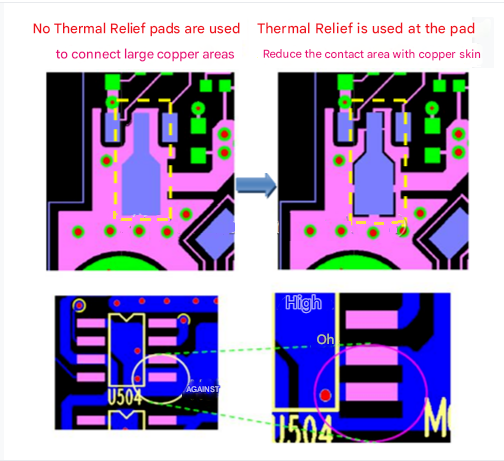
Comparison using Thermal Reliefpad
6.Check your work
When you are humming and humming to put all the parts together for manufacturing, it is easy to find problems at the end of the design project and be overwhelmed. Therefore, double and triple checking your design work at this stage can mean the difference between success and failure in manufacturing. To help complete the quality control process, we always recommend that you start with electrical rule checks (ERC) and design rule checks (DRC) to verify that your design fully meets all rules and constraints. With both systems, you can easily perform checks for gap widths, line widths, common manufacturing settings, high-speed requirements, shorts, and more. When your ERCs and DRCs produce error-free results, it is recommended that you check the routing of each signal, one signal line at a time from the schematic to the PCB to carefully confirm that you have not missed any information. Also, use the probing and shielding capabilities of your design tool to ensure that your PCB layout materials match your schematic.
Conclusion
When you have this – the top 5 PCB design guidelines that all our PCB designers need to know, by following these suggestions, you will soon be able to design functional and manufacturable boards with true quality printed circuit boards.
Good PCB design practices are essential to success, and these design rules lay the foundation for building and consolidating practical experience for continuous improvement in all design practices.