Transformer-Based Isolated Gate Driver Design for SiC MOSFET
This paper presents a transformer-based isolated gate driver for 3.3kV SiC MOSFET. Two VHF modulated resonant flyback converters operating at 20 MHz generate the PWM signals and gate drive power.
High voltage isolation characteristics (15 kV RMS) are provided by a PCB-based air-core transformer. The transformer has a low coupling capacitance of 5pF, which enhances noise immunity even under high dv/dt of SiC MOSFET. To evaluate the effectiveness of the proposed solution, experimental results for 3.3kV discrete SiC MOSFET are presented.
Isolated Gate Driver
The typical configuration of an isolated gate driver (GD) for high voltage SiC MOSFET is shown in Figure 1 (a). An isolated gate drive power supply (GDPS) is required, and optical fiber (OF) is usually used to transmit the gate PWM signal to ensure sufficient isolation and low parasitic capacitance on the signal path [1], [5]. The disadvantages of this solution are the high cost of optical fiber and the need for at least two isolated power supplies.
An alternative solution has been proposed based on a 20 kV isolated GDPS with a transformer based on PCB windings [2]. Although it has a low coupling capacitance (<2 pF), it results in a bulky transformer due to the gap distance between the magnetic core and the PCB windings.
Wireless power transfer (WPT) converters [3], [5] and GDPS based on optical power transfer [3], [4] allow you to eliminate the coupling capacitance but achieve low transmission power (<1 W) and conversion efficiency (<25%). Inductive power transfer GDPS uses a single-turn primary winding to power multiple secondary receivers [5], where the low coupling capacitance is achieved by a wide air gap between the primary winding and the magnetic core. However, if the primary transmitter fails, all secondary side gate voltages will be out of control.
The novel solution proposed in this paper is shown in Figure 1(b). By using a PCB-based air-core transformer with high dielectric strength, a 15 kV RMS insulation voltage is achieved. In addition, the low coupling capacitance enhances the noise immunity of the 3.3kV SiC MOSFET to high dv/dt.
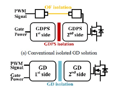
Figure 1: Conventional and Proposed Isolated GD Solutions
Schematic
The schematic diagram of the proposed solution is shown in Figure 2. On the primary side, the PWM signal is modulated with a VHF signal (20 MHz) to generate gate signals for two RFCs. The first RFC is active when the PWM signal is high (1), while the second is active when the PWM signal is low (0). The output voltage V O of both stages maintains a constant DC value regardless of the PWM duty cycle. Therefore, the power received on the secondary side is independent of the PWM duty cycle.
On the secondary side, two envelope detectors are connected to the anodes of diodes DR1 and DR2 to detect the ON/OFF state of the RFCs. These edge detection signals are then buffered as PWM rising and falling edges and sent to the RS bistable, which regenerates the PWM signal. The non-isolated DC-DC regulator connected after RFC 1 provides the required +5V, +15V, and -5V drive voltages for the secondary-side signal processing circuit.
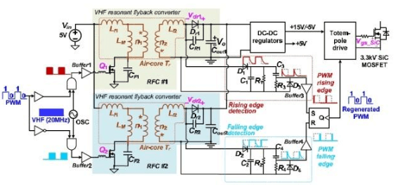
Figure 2: Schematic diagram of the proposed GD solution
The relevant waveforms are shown in Figure 3.
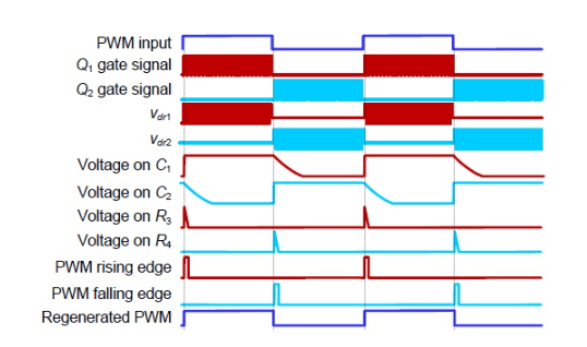
Figure 3: Key waveforms of the proposed GD
Transformer
The design of the PCB-based air-core transformer has the advantage of eliminating core losses and potential insulation issues between the winding and the core, as shown in Figure 4. It adopts a stacked PCB structure, including the primary PCB, transformer (Tr)-PCB, and secondary PCB. The transformer winding has a spiral shape to simplify the design. The Tr-PCB board has only two layers, with the primary and secondary windings on the top and bottom layers, respectively. With this solution, the insulation properties are completely provided by the dielectric material of the Tr-PCB board, which is typically low-cost FR-4.
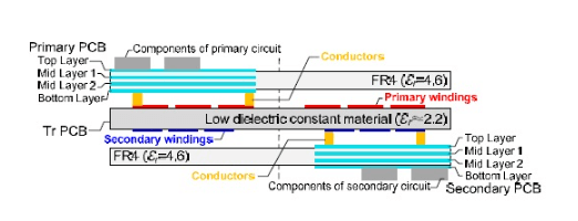
Figure 4: Structure of PCB-based transformer
To increase the dielectric breakdown voltage and reduce the coupling capacitance, materials with high dielectric strength and low dielectric constant can be used. The authors used Arlon-DiClad-880 material, which has a dielectric constant of 2.2 and a dielectric strength of more than 45kV/mm. The simulated coupling capacitance determined with the help of the Ansys Q3D extractor tool is about 5 pF for several transformers.
The creepage distance between the coated primary and secondary windings is higher than 30 mm × 2. This ensures an insulation voltage of 15 kV RMS according to the IEC-61800-5-1-2007 standard.
Experimental Results
Figure 5 shows the schematic diagram of the prototype used for testing, which was built in the lab using the components listed in Table I.
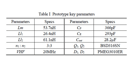
Table I: List of Components Used in the Prototype
SiC MOSFET Isolated Gate Driver with PCB-Based Transformer
Figure 5: Schematic Diagram of Prototype
The maximum output power of the RFC is measured at 1.5W@17Ω resistive load, which is sufficient to drive a 3.3kV SiC MOSFET (GR40MT33N). The graph of efficiency and RFC output voltage (V O ) is shown in Figure 6. Both RFCs maintain stable output characteristics over the entire load range (0.12W-1.5W).
SiC MOSFET Isolated Gate Driver with PCB-Based Transformer
Figure 6: Efficiency and RFC Output Voltage
In addition, a double pulse test (DPT) is implemented to evaluate the performance of the proposed GD. The schematic diagram of the DPT test bench is shown in Figure 7.
SiC MOSFET isolated gate driver with PCB-based transformer
Figure 7: Schematic diagram of DPT test bench
GD drives switch S1, where insulation voltage and noise immunity to high dv/dtare are required. The DPT experimental waveforms at Vdc=2kV, id_S1,max=44A, Lload=1.3mH, Rgon/Rgoff=2.2Ω/5Ω are shown in Figure 8. It can be seen that the maximum dv/dt achieved by the 3.3kV SiC MOSFET corresponds to a safe value of 100V/ns. The same GD solution can also be used for other high-voltage SiC MOSFET devices.