Transforming Gerber Files into Functional PCB Layouts
Key Takeaways
Transforming Gerber files into functional PCB layouts is crucial in the world of PCB manufacturing. You should prioritize understanding the nuances of these file formats, as they serve as the blueprint for your designs. Different PCB manufacturing companies can interpret these files differently, influencing the overall quality and outcome of your project. To minimize complications and pcb manufacturing cost, it is essential to employ the right tools and software tailored for this conversion process.
Before diving into the conversion, ensure your designs are organized and thoroughly documented. This preparation not only streamlines your workflow but also mitigates potential errors during conversion. As you progress through these steps, take care to optimize every element for clarity and efficacy in your final PCB.
To achieve a successful transformation, consider seeking advice from established professionals in the industry who can guide you through any intricate challenges that arise during this process. Always remember that a well-structured layout can significantly affect your pcb manufacturing business outcomes and product viability.
"A proper foundation in design can save both time and resources when moving towards production."
Ultimately, keeping an eye on revising and fine-tuning PCB layouts will lead you closer to achieving a design ready for production while ensuring that it aligns with current standards in pcb manufacturing. If you’re seeking reliable solutions, explore options that companies like Andwin PCB provide for streamlining this conversion journey.
Understanding Gerber Files: An Overview
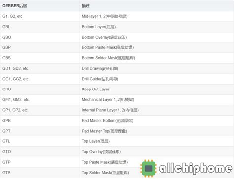
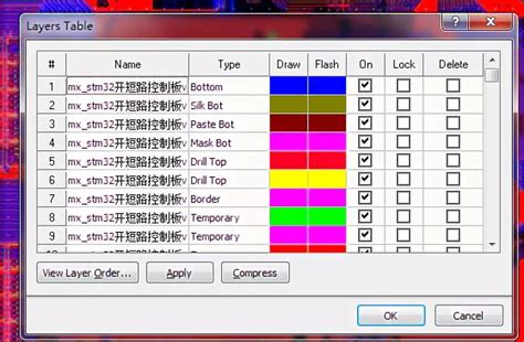
When working in the realm of PCB manufacturing, it is crucial to understand Gerber files, which serve as the standard format for PCB design data. These files are generated by PCB design software and contain vital information about the layer visuals, such as traces, pads, and vias. By grasping how to interpret and manipulate these files, you set a strong foundation for creating your own PCB layouts. Each layer in the Gerber file corresponds to different functions in the manufacturing process, from copper layers to silkscreen markings. This understanding can significantly impact your efficiency when collaborating with PCB manufacturing companies or handling the PCB manufacturing cost effectively. Familiarity with these files helps you to avoid common pitfalls that can arise during the transition from design to reality, ensuring that your PCB manufacturing business runs smoothly. By recognizing the elements within Gerber files, you can confidently step into more complex stages of layout conversion and ultimately achieve a higher-quality product that meets your specifications and those of your clients.
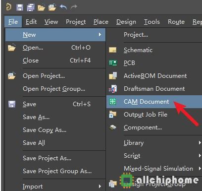
Essential Tools and Software for Conversion
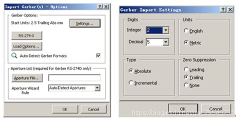
To successfully transform Gerber files into functional PCB layouts, having the right tools and software is crucial. Numerous software packages can assist you in this conversion process, making it easier to navigate the complexities of PCB manufacturing. For instance, popular platforms include Altium Designer, Eagle, and KiCAD. These tools not only allow for efficient layout design but also facilitate verification against design rules, ensuring your files meet the standards required by various PCB manufacturing companies.
When choosing a software solution, consider factors such as user interface, compatibility, and support resources. Here’s a brief overview of different tools with their respective features:
| Tool | Features | Cost |
|---|---|---|
| Altium Designer | Comprehensive features, user-friendly | High (Subscription) |
| Eagle | Flexible licensing, good community support | Moderate (Personal license available) |
| KiCAD | Open-source, customizable | Free |
Additionally, ensure that the software can accurately interpret different formats of Gerber files, as compatibility may vary. Effective utilization of these tools can significantly reduce the PCB manufacturing cost by minimizing errors in layout conversions and expediting the overall design process. Therefore, integrating modern software into your workflow not only streamlines the conversion but also bolsters your position within the competitive landscape of the PCB manufacturing business. By leveraging these essential resources, you enhance your capability to produce reliable and high-quality PCBs efficiently.
Preparing to Convert Gerber Files to PCB Layouts
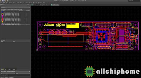
Before diving into the process of converting your Gerber files into functional PCB layouts, it’s essential to prepare adequately. Start by ensuring that you have the right tools and software at your disposal. Software capable of handling Gerber files, such as PCB design software, will not only facilitate the conversion but also help you visualize the layout effectively. Understanding the specific requirements of your project is crucial; consider aspects like the complexity of your design, layer count, and specific components required for your PCB manufacturing.
Moreover, familiarizing yourself with different PCB manufacturing companies and their capabilities can guide you in selecting one that aligns with your project needs. Take time to analyze various options concerning cost, materials, and production timeframes, as these factors significantly influence the overall PCB manufacturing cost. Ensuring that all design files are up to date will help minimize headaches later in the production phase. Remember, a well-structured process at this preparation stage can significantly impact the success of your PCB manufacturing business—setting a solid foundation for the conversion ahead.
Step-by-Step Guide to Transforming Gerber Files
When you start the journey of transforming Gerber files into practical PCB layouts, it’s crucial to follow a systematic approach to ensure efficiency and accuracy. Begin by selecting the right PCB manufacturing tools and software available in the market. Many of these can automate parts of the process, ultimately reducing both pcb manufacturing cost and time. As you prepare for conversion, ensure that your original designs are clean and well-documented, as this will ease the transfer into a layout format suitable for fabrication.
Next, methodically analyze each component represented in your Gerber files. This includes checking for details such as layer configurations, drill hole placements, and trace widths. These elements play a significant role in how your final layout will be interpreted by various pcb manufacturing companies. You’ll also want to use software capable of generating specific design rules that align with accepted standards in your PCB manufacturing business.
As you officially start your transformation, remember that meticulous verification at each stage can minimize errors during the entire conversion process. If inconsistencies arise, identifying them early can save you from costly mistakes at later stages of production. Thus, implementing checks throughout this step-by-step procedure is vital for a successful outcome when you eventually move toward the manufacturing phase. The effort put into properly translating Gerber data today can yield significant benefits for both functionality and cost-effectiveness in your upcoming production runs.
Minimizing Errors During the Conversion Process
When converting Gerber files into functional PCB layouts, ensuring accuracy is paramount to avoid costly revisions and delays in your PCB manufacturing projects. One major strategy for minimizing errors is to use reliable software tools that verify your designs during the conversion process. These tools often feature built-in error-checking capabilities that can catch common mistakes before they escalate. It’s also beneficial to maintain clear documentation of your original designs, as this will provide a point of reference throughout the conversion. Pay close attention to details such as layer alignment and component placement; even minor discrepancies can lead to significant challenges in the PCB manufacturing cost and timelines. Additionally, double-check your design rules and specifications specific to your targeted PCB manufacturing companies, as these often differ by provider. By employing these strategies, you can streamline your workflow and improve the efficiency of transforming Gerber files into high-quality PCB layouts, ultimately benefiting your overall business in the competitive landscape of PCB manufacturing.
Revision and Optimization: Fine-Tuning Your PCB Layout
Once you have transferred your Gerber files into a functional PCB layout, the next crucial step is revision and optimization. This phase is essential to ensure the efficiency and effectiveness of your design before it moves forward into PCB manufacturing. Begin by scrutinizing the layout for any possible errors or inefficiencies, such as trace widths that may not meet current standards or component placement that could lead to signal interference. It’s your responsibility to make certain that all connections are correct and that the design flow aligns with the specifications necessary for PCB manufacturing companies.
Additionally, consider revisiting the PCB manufacturing cost associated with various components and layout decisions. Optimizing your layout can not only improve performance but may also reduce costs significantly by simplifying connections and minimizing material use. Reducing layers where possible or revising routing paths might lead to a more economical design, which is a vital aspect when entering the competitive realm of PCB manufacturing business. Remember, every choice you make in this stage will have implications for production efficiency as well as overall product quality. Therefore, invest time in this phase; it will pay dividends when you’re ready to send your layout off for production.
Preparing for Manufacturing: What to Know Before Sending Your PCB
Before you finalize and send your PCB design files to PCB manufacturing companies, it’s essential to ensure that you have considered all critical aspects of the manufacturing process. First, verify that your Gerber files are accurate and complete, as these files are the backbone of your production. Missing or incorrect data can lead to increased PCB manufacturing costs or rework, ultimately delaying your project timeline.
It’s also wise to familiarize yourself with the specific capabilities of potential PCB manufacturing companies. Different manufacturers may offer varying technologies, materials, and tolerances that could affect both the performance and cost efficiency of your boards in production. Additionally, evaluate their lead times because quick-turn solutions may demand higher premiums but can be invaluable for urgent projects in a competitive PCB manufacturing business.
Furthermore, consider how your design adheres to standard practices for manufacturability. Ensuring that your layout meets industry standards not only streamlines communication with the manufacturer but also minimizes the potential for errors during assembly. This step is crucial for keeping costs low and ensuring that your final product meets both functionality and aesthetic requirements.
In summary, investing time upfront in preparing your PCB files can lead to smoother interactions with manufacturers and ultimately contribute to a more successful outcome for your project. Always remember that an informed approach will significantly reduce risks associated with PCB manufacturing, making sure you stay within budget and schedule constraints while delivering a high-quality product.
Tips for Analyzing and Updating Your Designs
When it comes to refining your PCB layouts, understanding the nuances of your designs is crucial. Start by conducting a thorough analysis of your existing design files. This includes reviewing the Gerber files to ensure that all layers are accounted for and properly aligned. As you progress, consider utilizing specialized tools that can help visualize different aspects of the layout clearly. If you’re part of a pcb manufacturing business, keeping track of any changes made during this phase is essential in preventing future issues.
Updating your designs requires a careful examination of each component’s placement and function within the overall design. Be mindful of the potential impact that changes may have on the pcb manufacturing cost; optimizing layout efficiency can lead to significant savings when partnering with pcb manufacturing companies. Additionally, this is an excellent opportunity to integrate modern design practices such as minimizing trace lengths and enhancing thermal management, which in turn can elevate the performance of your final product.
Finally, regularly engaging in this analytic process not only aids in perfecting current projects but also fosters an environment of continuous improvement that can greatly benefit your overall strategy in pcb manufacturing. Keeping your designs up-to-date with industry standards will help maintain product relevance while sustaining competitive advantage in a fast-evolving market.
Conclusion
In this journey of transforming Gerber files into functional PCB layouts, you have navigated the complexities that often arise during this process. Remember, the foundation of effective PCB manufacturing lies in understanding your designs and ensuring precision at every step. Avoiding common pitfalls is essential, as errors can significantly impact pcb manufacturing cost and turnaround times. It’s wise to engage with trusted pcb manufacturing companies that can provide both quality and reliability, ensuring your designs move seamlessly from conception to production. By staying informed about the latest trends and technologies in the pcb manufacturing business, you can better select tools and services that align with your project needs. As you prepare to send your finalized layouts for production, keep in mind that thorough preparation is key to minimizing setbacks and maximizing efficiency—ultimately leading to a successful product launch.
FAQs
What are Gerber files, and why are they important in PCB manufacturing?
Gerber files serve as the standard file format for representing the design of printed circuit boards (PCBs). They contain detailed information about the board layers, including copper traces, solder masks, and component placements. Understanding how to work with Gerber files is crucial for effective pcb manufacturing because they ensure that the designs are accurately translated into physical boards.
How do I choose the right PCB manufacturing companies?
When selecting pcb manufacturing companies, consider factors such as their reputation, production capabilities, pricing, and lead times. It’s essential to research customer reviews and ask for samples of their previous work to evaluate quality. Ensuring that the company has experience with similar projects can also help streamline your design process.
What factors influence PCB manufacturing cost?
Several factors can affect pcb manufacturing cost, including material type, layer count, size of the board, complexity of the design, and production volume. High-quality materials or advanced technologies like HDI boards may increase costs. Therefore, it’s important to outline your requirements clearly to receive accurate quotations from manufacturers.
What is involved in starting a PCB manufacturing business?
To start a pcb manufacturing business, you need to conduct market research and develop a solid business plan. Consider investments in equipment and technology essential for production. Building relationships with suppliers for materials and establishing partnerships with clients will be vital as you grow your business.
How can I minimize errors during the transition from Gerber files to PCB layouts?
Using reliable software tools during conversion helps minimize errors when transitioning from Gerber files to PCB layouts. Always double-check designs for inconsistencies and run electrical rule checks (ERC) within your CAD tools before finalizing layouts. Keeping detailed documentation can also help in identifying potential issues early on.


