Transparent PCB Boards: The Future of Electronics
Introduction
The world of electronics is constantly evolving, with new technologies emerging to meet the demands of modern applications. One such innovation that has garnered significant attention in recent years is the transparent printed circuit board (PCB). Transparent PCBs are a groundbreaking development in the field of electronics, offering a unique combination of functionality and aesthetics. These boards are not only visually appealing but also provide a range of technical advantages that make them suitable for a variety of applications, from consumer electronics to advanced medical devices.
This article delves into the concept of transparent PCBs, exploring their design, manufacturing process, advantages, challenges, and potential applications. By the end of this discussion, it will be clear why transparent PCBs are poised to play a pivotal role in the future of electronics.
What is a Transparent PCB?
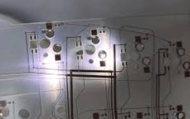
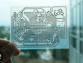
A transparent PCB is a type of printed circuit board that allows light to pass through its substrate, making it see-through. Unlike traditional PCBs, which are typically made from opaque materials like fiberglass (FR4) or phenolic resin, transparent PCBs use materials such as glass, polyimide, or transparent polymers as their base. The conductive traces on these boards are often made from transparent conductive materials like indium tin oxide (ITO) or silver nanowires, which maintain electrical conductivity while remaining visually unobtrusive.
The transparency of these boards opens up new possibilities for design and functionality, particularly in applications where aesthetics or light transmission are critical. For example, transparent PCBs are increasingly being used in wearable technology, display systems, and smart windows.
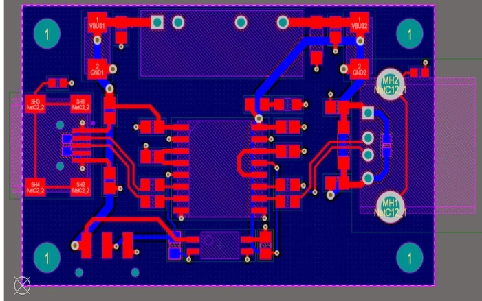
Design and Manufacturing Process
The design and manufacturing of transparent PCBs involve several unique steps compared to traditional PCBs. Here’s an overview of the process:
- Material Selection: The choice of substrate is critical in transparent PCB manufacturing. Common materials include glass, polyimide, and transparent polymers like polyethylene terephthalate (PET) or polyethylene naphthalate (PEN). These materials must be optically clear, thermally stable, and mechanically robust.
- Conductive Layer Deposition: The next step is to deposit a transparent conductive layer onto the substrate. Indium tin oxide (ITO) is the most widely used material for this purpose due to its excellent conductivity and transparency. However, alternatives like silver nanowires, graphene, and conductive polymers are also being explored.
- Patterning and Etching: The conductive layer is then patterned to create the desired circuit layout. This is typically done using photolithography or laser etching techniques. The goal is to create precise, fine-line traces that are both electrically functional and visually transparent.
- Component Assembly: Once the circuit pattern is complete, electronic components are mounted onto the board. This can be done using surface-mount technology (SMT) or through-hole technology, depending on the design requirements.
- Encapsulation and Finishing: To protect the circuit and ensure durability, the board is often encapsulated with a transparent protective layer. This step also enhances the board’s optical clarity and resistance to environmental factors like moisture and dust.
Advantages of Transparent PCBs
Transparent PCBs offer several advantages over traditional opaque PCBs, making them an attractive option for a wide range of applications:
- Aesthetic Appeal: The see-through nature of these boards allows for sleek, modern designs that are particularly appealing in consumer electronics. For example, transparent PCBs can be used in smartphones, smartwatches, and other devices to create a futuristic look.
- Light Transmission: In applications like LED displays, smart windows, and optical devices, the ability to transmit light is a critical feature. Transparent PCBs enable the integration of electronics without obstructing light flow.
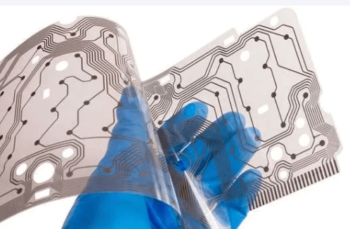
- Flexibility: Many transparent PCB materials, such as polyimide and PET, are flexible. This makes them ideal for use in wearable technology, foldable devices, and other applications where flexibility is required.
- Durability: Transparent PCBs made from materials like glass are highly durable and resistant to environmental factors such as heat, moisture, and corrosion.
- Innovative Applications: The unique properties of transparent PCBs open up new possibilities for innovation. For instance, they can be used in heads-up displays (HUDs), augmented reality (AR) devices, and even in medical imaging systems.
Challenges and Limitations
Despite their many advantages, transparent PCBs also face several challenges that need to be addressed for widespread adoption:
- Cost: The materials and manufacturing processes used for transparent PCBs are often more expensive than those for traditional PCBs. For example, ITO is a costly material, and the precision required for patterning and etching adds to the overall cost.
- Conductivity Limitations: While materials like ITO offer good conductivity, they are not as conductive as traditional metals like copper. This can limit the performance of transparent PCBs in high-power applications.
- Manufacturing Complexity: The production of transparent PCBs requires specialized equipment and expertise, which can be a barrier for smaller manufacturers.
- Durability Concerns: Although glass-based transparent PCBs are durable, polymer-based boards may be more susceptible to scratching and wear over time.
- Thermal Management: Transparent materials often have different thermal properties compared to traditional PCB materials, which can pose challenges in managing heat dissipation.

Applications of Transparent PCBs
Transparent PCBs are finding use in a variety of industries and applications, thanks to their unique properties. Some of the most promising applications include:
- Consumer Electronics: Transparent PCBs are being used in smartphones, tablets, and wearable devices to create visually striking designs. For example, a transparent PCB could be used in a smartwatch to display information on a see-through screen.
- Displays and Lighting: In LED displays and lighting systems, transparent PCBs allow for efficient light transmission while integrating the necessary electronics. This is particularly useful in applications like OLED displays and automotive lighting.
- Smart Windows: Transparent PCBs are a key component in smart windows, which can change their opacity or display information. These windows are used in buildings, vehicles, and even in augmented reality applications.
- Medical Devices: In the medical field, transparent PCBs are being explored for use in imaging systems and diagnostic equipment. Their ability to transmit light makes them ideal for applications like endoscopy and optical sensors.
- Automotive Industry: Transparent PCBs are being integrated into heads-up displays (HUDs) and dashboard systems in modern vehicles. They provide a clear view of information while maintaining the sleek design of the car’s interior.
- Aerospace and Defense: The durability and lightweight nature of transparent PCBs make them suitable for use in aerospace and defense applications, such as cockpit displays and optical sensors.
Future Prospects
The future of transparent PCBs looks promising, with ongoing research and development aimed at overcoming current limitations and expanding their applications. Some key areas of focus include:
- Material Innovation: Researchers are exploring new materials that offer better conductivity, transparency, and durability. For example, graphene and carbon nanotubes are being investigated as potential alternatives to ITO.
- Cost Reduction: Advances in manufacturing techniques and economies of scale are expected to reduce the cost of transparent PCBs, making them more accessible for a wider range of applications.
- Integration with Emerging Technologies: Transparent PCBs are likely to play a key role in emerging technologies like flexible electronics, Internet of Things (IoT) devices, and 5G networks.
- Sustainability: As the electronics industry moves towards more sustainable practices, transparent PCBs made from recyclable or biodegradable materials could become a focus area.
Conclusion
Transparent PCBs represent a significant leap forward in the field of electronics, offering a unique combination of functionality and aesthetics. While there are challenges to overcome, the potential applications of these boards are vast and varied, spanning industries from consumer electronics to aerospace. As research and development continue, transparent PCBs are likely to become an integral part of the electronics landscape, driving innovation and enabling new possibilities for design and functionality.
In a world where technology is increasingly intertwined with our daily lives, transparent PCBs offer a glimpse into a future where electronics are not only powerful and efficient but also beautiful and seamlessly integrated into our environment. The journey of transparent PCBs is just beginning, and their impact on the electronics industry is sure to be profound.