Turnkey PCB Deployment Strategies for Accelerated Market Entry

Key Takeaways
Adopting turnkey PCB solutions bridges the gap between design and PCBA (printed circuit board assembly), enabling seamless transitions from concept to mass production. By unifying PCB assembly with prototyping and testing phases, businesses eliminate fragmented workflows, reducing lead times by up to 40%. Scalability becomes achievable through standardized processes, allowing manufacturers to adjust volumes without compromising quality control metrics.
A critical advantage lies in cost optimization: consolidated turnkey PCB services leverage economies of scale, trimming material waste and logistical overhead. For startups, rapid PCBA iterations shorten validation cycles, accelerating market entry by 6–8 weeks compared to traditional methods. Additionally, integrated quality assurance protocols—such as automated optical inspection (AOI)—ensure defect rates remain below 0.1%, aligning with industry benchmarks.
While conventional approaches often silo design, fabrication, and PCB assembly, turnkey providers synchronize these stages under one framework. This cohesion minimizes miscommunication risks and ensures compliance with regulatory standards like IPC-A-610. For enterprises targeting agile scaling, end-to-end solutions offer a competitive edge, balancing speed, precision, and adaptability in dynamic markets.
Turnkey PCB Design & Manufacturing Integration
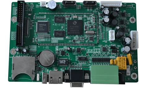
Integrated turnkey PCB solutions bridge the gap between design and production by unifying PCB assembly (PCBA) workflows under a single provider. This approach eliminates communication silos between design engineers and manufacturing teams, ensuring design-for-manufacturability (DFM) principles are embedded from the initial schematic phase. Advanced PCBA partners leverage automated design validation tools to flag potential fabrication issues, such as component spacing violations or thermal mismatches, before prototyping begins.
Tip: Prioritize vendors offering real-time DFM feedback during design reviews to avoid costly revisions post-prototyping.
By synchronizing PCB assembly processes with design intent, manufacturers reduce material waste by up to 22% and compress lead times by aligning component sourcing with production schedules. For instance, unified platforms enable just-in-time procurement of surface-mount devices (SMDs) based on finalized Gerber files, minimizing inventory overhead. This cohesion also supports seamless scaling—a critical advantage when transitioning from low-volume prototypes to high-volume runs.
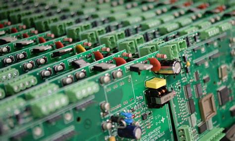
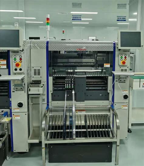
The integration of automated optical inspection (AOI) systems within turnkey PCB pipelines further ensures consistency across batches. Manufacturers employing closed-loop feedback between testing data and design software achieve <2% defect rates, even for complex multilayer boards. Such alignment not only accelerates market entry but also establishes a foundation for iterative product enhancements without disrupting production timelines.
Reducing Costs with Turnkey PCB Services
Adopting turnkey PCB services enables businesses to consolidate design, prototyping, and PCB assembly into a single workflow, eliminating fragmented vendor relationships and redundant costs. By partnering with a turnkey PCBA provider, companies avoid the logistical overhead of coordinating multiple suppliers, which often leads to miscommunication, delays, and inflated expenses. For instance, integrated material procurement reduces bulk purchasing gaps, while standardized processes minimize rework rates and waste generation.
| Cost Factor | Traditional Approach | Turnkey Solution |
|---|---|---|
| Vendor Management | 3-5 separate contracts | Single-point accountability |
| Prototyping Iterations | 4-6 cycles (avg.) | 2-3 cycles (avg.) |
| Material Sourcing | Inconsistent pricing tiers | Pre-negotiated supplier discounts |
The economies of scale achieved through turnkey PCBA workflows also lower per-unit costs, particularly for mid-to-high volume production. Automated design validation tools further reduce human error risks, ensuring compliance with specifications early in the process. Additionally, transparent pricing models eliminate hidden fees tied to PCB assembly, such as tooling charges or expedited shipping premiums. By aligning prototyping and mass production under one provider, businesses can reallocate resources toward innovation rather than operational overhead, maintaining budget predictability without sacrificing quality.
This approach not only addresses immediate cost challenges but also supports scalability, as suppliers optimize processes for future expansions. Transitioning to a unified model ensures that savings from streamlined PCB assembly directly contribute to accelerated market entry—a critical advantage in competitive industries.
Accelerate Market Entry Through PCB Prototyping
Rapid prototyping serves as the cornerstone for compressing development timelines in electronics manufacturing. By leveraging PCB assembly (PCBA) services within turnkey frameworks, companies can validate designs before committing to full-scale production, minimizing costly revisions. Advanced PCBA partners utilize automated design-for-manufacturability (DFM) checks during prototyping, identifying potential flaws in circuitry, component placement, or thermal management early in the process. This iterative approach reduces time-to-market by 30–50% compared to traditional sequential workflows, according to industry benchmarks.
Integrated turnkey systems synchronize prototyping with material procurement and testing protocols, enabling parallel development of firmware and mechanical enclosures. For instance, high-density interconnect (HDI) prototypes produced through automated PCB assembly lines allow engineers to stress-test signal integrity under real-world conditions. Such precision ensures scalability when transitioning to volume manufacturing, as process parameters are already optimized. Additionally, turnkey providers often bundle functional testing and compliance certification with prototyping phases, further eliminating bottlenecks.
By aligning prototyping cycles with PCBA readiness, businesses mitigate risks associated with component obsolescence or supply chain delays—a critical advantage in fast-moving sectors like IoT or automotive electronics. This strategy not only accelerates market entry but also establishes a foundation for seamless scaling, as validated prototypes directly inform mass-production workflows.
Scalable Turnkey PCB Production Solutions
Modern electronics manufacturers increasingly prioritize scalable turnkey PCB production solutions to align with fluctuating market demands. By integrating PCB assembly (PCBA) workflows with automated design validation tools, companies can seamlessly transition from prototyping to mass production. This approach eliminates bottlenecks in component sourcing, material traceability, and testing protocols, ensuring consistent quality across batches. Advanced turnkey services leverage modular manufacturing frameworks, enabling rapid adjustments to production volumes without sacrificing efficiency or incurring redundant costs.
A critical advantage lies in the synchronization of PCB design and PCBA processes, which minimizes rework by addressing potential compatibility issues early. For instance, design-for-manufacturability (DFM) checks embedded within the workflow reduce assembly errors by up to 40%, according to industry benchmarks. Additionally, partnerships with certified suppliers streamline material procurement, while IoT-enabled monitoring systems provide real-time insights into yield rates and defect trends. Such scalability not only supports short-run batches for niche markets but also accommodates high-volume orders through flexible line configurations. By embedding agility into every stage—from prototyping to final PCB assembly—businesses can dynamically respond to market shifts while maintaining cost-efficiency and technical compliance.
Quality Control in Turnkey PCB Deployment
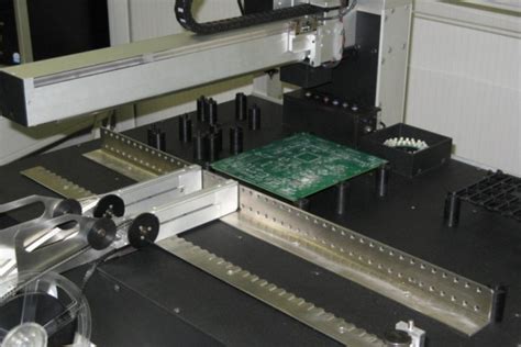
Effective quality control mechanisms form the backbone of successful turnkey PCB deployment, ensuring seamless integration of PCB assembly (PCBA) processes from design to delivery. Advanced inspection protocols, such as automated optical inspection (AOI) and X-ray testing, are embedded at critical stages to identify defects in solder joints, component placement, or trace integrity. By aligning PCB assembly workflows with statistical process control (SPC) methodologies, manufacturers achieve ≤0.1% defect rates while maintaining compliance with IPC-A-610 and ISO 9001 standards.
Real-time data analytics further enhance traceability, enabling rapid root-cause analysis during PCBA production. For instance, thermal profiling during reflow soldering is optimized to prevent delamination or warping, directly impacting long-term reliability. Scalability is preserved through standardized testing frameworks, such as in-circuit testing (ICT) and functional validation, which adapt to varying batch sizes without compromising turnaround times. This systematic approach not only mitigates risks of post-deployment failures but also reinforces client trust in end-to-end turnkey solutions—a critical factor for accelerating market entry in competitive industries.
Streamlining PCB Development for Faster Launches
Efficient PCB assembly processes are critical for compressing development timelines without compromising reliability. By adopting design for manufacturability (DFM) principles early in the development cycle, teams can identify potential bottlenecks in PCBA workflows, such as component placement conflicts or thermal management issues. Advanced design tools, coupled with simulation software, enable rapid iteration, reducing rework during prototyping. For instance, integrating automated optical inspection (AOI) systems in PCB assembly lines ensures real-time defect detection, accelerating validation phases by up to 40%.
A unified approach to PCBA development—combining design, prototyping, and volume production under one framework—eliminates handoff delays between siloed teams. This cohesion is particularly vital for high-mix, low-volume applications, where scalability hinges on flexible manufacturing protocols. Transitioning from prototype to mass production becomes seamless when using standardized materials and modular tooling, which cuts lead times by 25–30%. Additionally, partnering with turnkey providers offering concurrent engineering support ensures that design adjustments align with PCB assembly capabilities, further trimming time-to-market.
To maintain momentum, teams should prioritize supplier collaboration, leveraging shared data platforms for real-time feedback on component availability and manufacturability. This proactive strategy minimizes pauses caused by redesigns or part shortages, ensuring that streamlined development translates directly into faster product launches.
Turnkey vs Traditional PCB Manufacturing Approaches
When evaluating PCB manufacturing methodologies, the distinction between turnkey and traditional approaches becomes critical for project success. Turnkey PCB services unify design, prototyping, PCB assembly (PCBA), and testing under a single provider, eliminating fragmented workflows inherent in traditional models. In contrast, conventional methods often require coordinating multiple vendors for tasks like component procurement, fabrication, and PCBA, introducing delays and miscommunication risks.
A key advantage of turnkey solutions lies in their end-to-end accountability. By consolidating processes such as PCB assembly and quality assurance, manufacturers reduce cross-vendor handoffs, minimizing errors and accelerating timelines. Traditional setups, while offering modular flexibility, demand significant internal oversight for tasks like bill of materials (BOM) validation and supply chain alignment—resources that could otherwise focus on innovation.
Cost structures also diverge: turnkey models leverage bulk material purchasing and standardized workflows to optimize pricing, whereas traditional approaches often incur hidden expenses from logistical gaps or rework. For complex projects requiring rapid scaling—such as multilayer boards or HDI designs—turnkey PCBA services provide built-in scalability without compromising design integrity. However, traditional methods retain relevance for highly specialized, low-volume applications where bespoke engineering takes precedence over speed.
Ultimately, the choice hinges on balancing speed, cost, and control. Turnkey PCB deployment streamlines market entry for time-sensitive products, while traditional frameworks cater to niche requirements demanding granular oversight.
End-to-End PCB Solutions for Rapid Scaling
Implementing end-to-end PCB solutions enables businesses to transition seamlessly from prototyping to high-volume production, addressing scalability challenges inherent in electronics manufacturing. By integrating PCB assembly (PCBA) workflows with design and testing phases, manufacturers eliminate bottlenecks caused by fragmented processes. A unified approach ensures consistent material sourcing, automated testing protocols, and real-time data sharing across teams—critical for maintaining quality while scaling output.
Turnkey PCBA providers optimize supply chain logistics, leveraging pre-vetted component libraries and bulk procurement to reduce lead times by up to 40%. This integration minimizes risks of mismatched specifications, which often delay traditional manufacturing models. For instance, combining design-for-manufacturability (DFM) analysis with automated assembly lines allows rapid adjustments to production volumes without compromising reliability.
Additionally, scalable PCB solutions incorporate modular infrastructure, enabling manufacturers to pivot between low-mix/high-volume and high-mix/low-volume demands. Advanced traceability systems further enhance agility by tracking components from procurement to final testing, ensuring compliance with industry standards. Such end-to-end frameworks not only accelerate time-to-market but also future-proof operations against evolving technological or market shifts.
Conclusion
Adopting turnkey PCB solutions represents a strategic imperative for businesses aiming to optimize product development cycles while balancing cost-efficiency and scalability. By integrating PCB assembly (PCBA) workflows with end-to-end design and manufacturing processes, companies eliminate fragmented workflows that traditionally delay time-to-market. Advanced turnkey providers leverage automated design verification and rapid prototyping to compress development phases, ensuring seamless transitions from concept validation to mass production. This holistic approach not only mitigates risks associated with component sourcing and PCBA quality but also enables real-time adjustments to meet evolving market demands. Furthermore, standardized quality assurance protocols embedded within turnkey PCB ecosystems ensure consistent output, even as production scales. For innovators prioritizing agility, the shift from siloed traditional manufacturing to unified turnkey frameworks offers a competitive edge—transforming complex technical processes into predictable, accelerated pathways for commercial success.
Frequently Asked Questions
How do turnkey PCB services differ from traditional manufacturing approaches?
Turnkey solutions integrate PCB assembly (PCBA), design, and prototyping under one provider, eliminating fragmented workflows. Traditional methods often require coordinating multiple vendors, increasing lead times and risks of miscommunication.
What cost advantages do turnkey PCB assembly offer?
By consolidating design, PCBA, and testing, turnkey providers reduce material waste, logistics overhead, and redundant labor. Bulk purchasing power and standardized processes further drive down unit costs while maintaining scalability.
Can turnkey strategies accelerate prototyping phases?
Yes. Unified teams streamline feedback loops, enabling rapid iterations. For example, design flaws identified during PCB assembly can be resolved in real time, avoiding weeks of delays common in fragmented workflows.
How is quality ensured in turnkey PCB deployment?
Reputable providers implement automated optical inspection (AOI), functional testing, and IPC-compliant processes. Centralized accountability minimizes quality gaps, as the same team oversees design validation, PCBA, and final inspections.
Are turnkey solutions scalable for high-volume production?
Absolutely. Modular workflows allow seamless transition from prototypes to mass manufacturing. Providers leverage advanced equipment and certified materials to maintain consistency across batches, whether producing 100 or 100,000 units.
Explore Custom Turnkey PCB Solutions Today
Ready to streamline your product’s journey from concept to market? Click here to discover how our end-to-end PCB assembly services can accelerate your deployment timeline.