Turnkey PCB Manufacturing Solutions for Rapid Prototyping Success
Key Takeaways
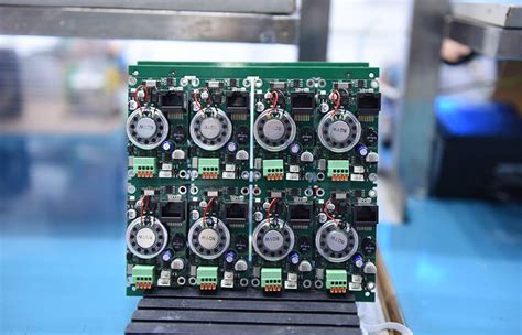
Implementing turnkey PCB solutions begins with understanding how integrated workflows bridge design, PCB assembly, and testing phases. By consolidating these stages under a single provider, teams eliminate logistical bottlenecks that often delay prototyping. For instance, PCBA (Printed Circuit Board Assembly) processes benefit from synchronized material procurement and automated assembly lines, reducing lead times by up to 40%.
A critical advantage lies in balancing speed with precision. Advanced turnkey services employ design-for-manufacturing (DFM) analysis to preempt errors, ensuring prototypes meet exact specifications. Consider the following comparison of traditional vs. turnkey approaches:
| Factor | Traditional Approach | Turnkey Solution |
|---|---|---|
| Component Sourcing | Multi-vendor | Single-point procurement |
| Assembly Lead Time | 10–15 days | 5–7 days |
| Cost Transparency | Variable | Fixed pricing |
To maximize cost-efficiency, prioritize suppliers offering scalable PCB assembly volumes and real-time project tracking. Best practices include adopting standardized component libraries and leveraging automated optical inspection (AOI) during PCBA to minimize rework. These strategies not only accelerate timelines but also align with rigorous quality benchmarks, positioning teams for seamless product launches.
Streamline PCB Design-Delivery Workflows
Modern electronics development demands seamless coordination between design and manufacturing phases. By integrating PCB assembly (PCBA) processes with advanced design tools, engineers can eliminate bottlenecks that traditionally delay prototyping. Automated design-for-manufacturability (DFM) checks, for example, flag potential issues in real-time, enabling rapid iterations without compromising precision. Cloud-based collaboration platforms further synchronize stakeholders, ensuring schematic updates instantly reflect in production-ready files.
A robust turnkey PCB approach merges PCB design, fabrication, and PCBA into a unified workflow, reducing manual handoffs by up to 40%. This integration is critical for applications requiring strict compliance, such as medical devices or automotive systems, where even minor discrepancies risk costly redesigns. Leveraging services like Rocket PCB’s design solutions ensures adherence to industry standards while accelerating time-to-market.
To optimize efficiency, standardized protocols like IPC-6012 and automated component sourcing minimize errors during PCB assembly. Real-time tracking systems provide visibility into material availability and production milestones, allowing teams to preempt delays. By aligning design intent with manufacturing capabilities early, companies achieve first-pass success rates exceeding 90%, slashing development cycles and unlocking faster product launches.
Accelerate Prototyping With Turnkey Solutions
By integrating PCB assembly and PCBA processes into a unified workflow, turnkey solutions eliminate fragmented coordination between design, fabrication, and testing stages. This cohesive approach reduces lead times by up to 40%, enabling engineers to iterate designs faster while maintaining precision and repeatability. For instance, automated component sourcing and real-time DFM (Design for Manufacturability) checks minimize errors that typically delay prototyping cycles.
A critical advantage lies in leveraging turnkey PCB manufacturing partners who manage everything from material procurement to final inspection. This eliminates vendor handoffs, ensuring seamless communication and faster resolution of design ambiguities. Recent industry insights highlight how combining PCBA expertise with advanced prototyping tools can compress development timelines by aligning electrical and mechanical validation phases.
Additionally, standardized testing protocols embedded within turnkey workflows—such as automated optical inspection (AOI) and functional testing—ensure prototypes meet production-grade quality benchmarks. By outsourcing logistical complexities, teams focus on innovation rather than supply chain coordination, accelerating time-to-market without compromising on cost-efficiency or performance reliability.
Ensure Precision in Rapid PCB Development
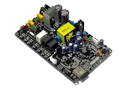
Achieving precision in PCB assembly requires a meticulous balance between advanced engineering practices and rigorous quality control. For rapid prototyping, even minor deviations in component placement or solder joint integrity can derail timelines and escalate costs. Modern turnkey solutions integrate automated optical inspection (AOI) and X-ray testing to detect defects as small as 10µm, ensuring PCBA outputs meet exact design specifications. By leveraging expert assembly services, teams gain access to real-time feedback loops that refine fabrication parameters, such as solder paste application and thermal profiling, to align with high-frequency or high-power applications.
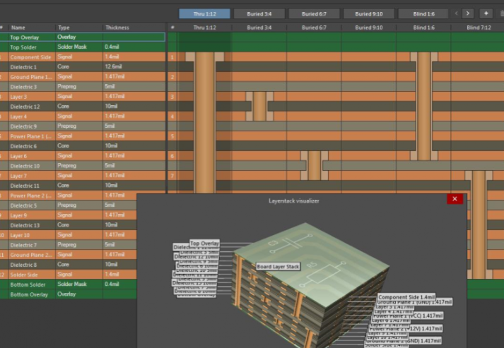
Critical to this process is the synchronization of design files with manufacturing capabilities. For instance, impedance-controlled routing and stack-up validation prevent signal integrity issues, while material selection (e.g., low-loss laminates) ensures reliability under stress. Advanced PCB assembly partners employ machine-learning algorithms to predict and mitigate potential failure points, reducing rework cycles by up to 40%. This approach not only accelerates iteration speed but also guarantees that prototypes mirror production-grade performance—a cornerstone for scaling innovations efficiently.
Maximize Cost-Efficiency in PCB Manufacturing
Achieving cost-efficiency in PCB manufacturing requires a strategic balance between design optimization, material selection, and process automation. Design-for-manufacturability (DFM) principles play a pivotal role here, enabling engineers to identify and eliminate potential inefficiencies early in the pcb assembly cycle. By aligning design specifications with production capabilities, teams can reduce rework, minimize material waste, and avoid costly delays.
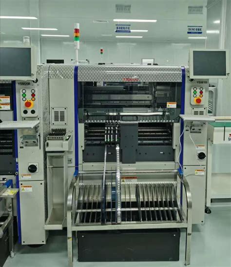
Leveraging pcba (printed circuit board assembly) automation further enhances cost savings. Advanced pick-and-place systems, solder paste inspection tools, and automated optical inspection (AOI) streamline workflows while maintaining high yield rates. Bulk purchasing of components through consolidated supplier partnerships also lowers per-unit costs, particularly for high-volume orders.
Another key consideration is the integration of testing phases directly into the pcb assembly process. In-circuit testing (ICT) and functional validation during pcba stages prevent post-production defects, reducing the financial impact of recalls or revisions. Additionally, adopting modular designs for multi-project panels optimizes material usage, cutting raw PCB fabrication expenses by up to 30%.
By prioritizing these strategies, businesses can achieve scalable cost reductions without compromising on quality—ensuring rapid prototyping success aligns seamlessly with long-term profitability goals.
Master Turnkey PCB Assembly Best Practices
Effective PCB assembly relies on harmonizing design intent with manufacturing realities. To achieve this, begin by conducting thorough design-for-manufacturability (DFM) checks, ensuring layouts align with PCBA production capabilities. Partnering with a trusted turnkey provider simplifies component sourcing, reducing lead times and mitigating supply chain risks. Prioritize automated optical inspection (AOI) and X-ray testing to detect soldering defects or misalignments early, preventing costly rework.
Optimize PCB assembly workflows by standardizing documentation—including Gerber files, bill of materials (BOM), and assembly drawings—to minimize ambiguity. For complex PCBA projects, leverage sequential solder reflow techniques or selective soldering to maintain integrity in mixed-technology boards. Implementing thermal management protocols during assembly ensures reliability, particularly for high-density or high-frequency designs.
Finally, align with manufacturers offering real-time progress tracking and proactive communication. This transparency allows rapid adjustments, ensuring timelines stay intact while preserving quality. By mastering these practices, teams transform PCB assembly from a bottleneck into a strategic accelerator for product development.
Optimize PCB Prototyping Speed and Quality
Achieving rapid PCB prototyping without compromising quality demands a harmonized approach to design validation, material selection, and pcb assembly workflows. By integrating automated design-for-manufacturing (DFM) checks early in the process, engineers can preemptively address potential bottlenecks in signal integrity or thermal management, reducing iterative delays. Advanced pcba (printed circuit board assembly) services leverage high-precision pick-and-place systems and reflow soldering technologies to ensure component placement accuracy, even for micro-BGA or QFN packages.
To accelerate timelines, opt for turnkey partners offering real-time collaboration between design and manufacturing teams, synchronizing schematic updates with fabrication readiness. For instance, combining pcb assembly with in-house testing—such as automated optical inspection (AOI) or X-ray verification—eliminates third-party dependencies, slashing lead times by up to 40%. Additionally, using standardized substrate materials with verified performance profiles minimizes risk during high-speed prototyping.
For teams prioritizing both speed and reliability, request a tailored quote to explore how integrated pcba solutions can align with your project’s technical and scheduling requirements. This end-to-end coordination ensures prototypes meet functional benchmarks while maintaining scalability for future production phases.
Strategies for Seamless PCB Product Launches
Achieving a successful product launch in the PCB assembly industry demands meticulous coordination between design, prototyping, and mass production. A turnkey approach simplifies this process by integrating PCBA design validation, component sourcing, and testing into a unified workflow. Start by aligning your design team with manufacturing partners early to identify potential bottlenecks—such as component lead times or layer stack-up complexities—that could delay timelines. Leverage advanced simulation tools to preemptively address signal integrity or thermal management issues, reducing iterative revisions during PCB assembly.
Collaboration with certified PCBA providers, like MIS Electronics, ensures access to just-in-time inventory systems and automated quality checks, critical for maintaining consistency across batches. Implement design for manufacturability (DFM) principles to minimize rework, such as optimizing pad sizes for automated soldering or avoiding high-density interconnects in cost-sensitive projects. For rapid scaling, prioritize suppliers offering flexible turnkey PCB solutions with transparent communication channels to track progress in real time.
Finally, validate prototypes under real-world conditions to uncover hidden flaws before full-scale production. By embedding risk-mitigation strategies—like dual-source component procurement and accelerated lifecycle testing—into your PCBA workflow, you can accelerate time-to-market while safeguarding product reliability. This holistic alignment of engineering rigor and supply chain agility transforms complex launches into predictable, repeatable successes.
Leverage Expert PCB Turnkey Service Benefits
Adopting PCB assembly expertise through turnkey services eliminates fragmented workflows, enabling seamless coordination from design validation to final PCBA testing. By integrating design-for-manufacturability (DFM) analysis and component sourcing under one roof, engineers mitigate risks of mismatched specifications or delayed material procurement. Specialized providers, such as Neuronic Works, leverage automated assembly lines and industry-certified processes to ensure consistent quality, even for high-mix, low-volume prototyping. This unified approach reduces PCB assembly lead times by up to 40%, while real-time progress tracking enhances transparency across stakeholders.
Moreover, turnkey partners optimize PCBA cost structures through bulk material purchasing and waste reduction strategies, directly benefiting projects with tight budget constraints. Advanced testing protocols, including in-circuit (ICT) and functional validation, further minimize post-production rework, accelerating time-to-market. For startups and enterprises alike, outsourcing to turnkey experts allows teams to focus on core R&D, secure in the knowledge that supply chain complexities and technical compliance are managed proactively. This strategic alignment ensures prototyping iterations align with market-ready standards, setting a foundation for scalable manufacturing transitions—a critical advantage in competitive electronics sectors.
Conclusion
Adopting turnkey PCB manufacturing solutions eliminates fragmented workflows by integrating PCB assembly (PCBA), testing, and logistics into a unified process. This approach ensures rapid prototyping cycles while maintaining cost-efficiency and precision, critical for accelerating product development timelines. By leveraging expert turnkey services, teams can mitigate risks associated with supply chain delays or design flaws, enabling seamless transitions from concept to market-ready products.
Tip: For optimal results, partner with providers offering end-to-end PCBA capabilities, including design validation and functional testing, to avoid costly revisions during scaling.
The synergy between advanced PCB assembly technologies and streamlined project management reduces time-to-market by up to 40%, according to industry benchmarks. Additionally, standardized workflows in turnkey solutions ensure consistency across batches, which is vital for high-volume production. As innovation accelerates, businesses prioritizing integrated manufacturing strategies will maintain competitive advantages in dynamic markets. Transitioning to a turnkey PCB model isn’t just about speed—it’s about building resilience through agile, data-driven processes that align with evolving industry demands.
Frequently Asked Questions
What distinguishes turnkey PCB manufacturing from traditional prototyping services?
A turnkey approach integrates PCB assembly (PCBA), component sourcing, and testing into a single workflow. This eliminates vendor coordination delays, ensuring rapid design iterations and faster time-to-market.
How do turnkey solutions ensure precision in high-speed prototyping?
Advanced DFM checks and automated optical inspection (AOI) are embedded in PCBA processes. Real-time collaboration between design and manufacturing teams minimizes errors, maintaining tight tolerances even under accelerated timelines.
Can cost-efficiency coexist with expedited PCB development?
Yes. By consolidating prototyping, PCB assembly, and logistics under one provider, material waste and overhead costs drop. Bulk purchasing of components and optimized panelization further enhance savings without compromising speed.
What quality controls are critical for rapid-turn PCB projects?
Multi-stage validations—including electrical testing, X-ray inspection, and functional verification—are standardized. For PCBA, in-circuit testing (ICT) ensures 98%+ first-pass yield, reducing rework cycles during time-sensitive builds.
How scalable are turnkey services for mass production after prototyping?
Seamless scalability is achieved through unified data management and pre-validated supply chains. Transitioning from 10 to 10,000 units requires minimal reconfiguration, as PCB assembly workflows are designed for volume flexibility.
Ready to Streamline Your Next Project?
For tailored turnkey PCB strategies that align with your prototyping goals, please click here to consult our engineering team.