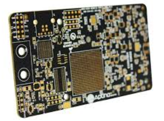
Ultra hdi pcb
Advances In Ultra HDI PCB Manufacturing Techniques
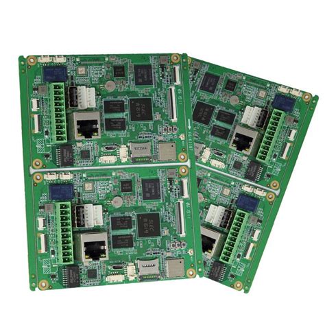
The field of printed circuit board (PCB) manufacturing has witnessed significant advancements over the years, with Ultra High-Density Interconnect (Ultra HDI) PCBs representing the pinnacle of this evolution.
These advanced PCBs are characterized by their ability to support higher component densities, finer lines and spaces, and smaller vias, which are essential for modern electronic devices that demand compactness and enhanced performance. The manufacturing techniques for Ultra HDI PCBs have evolved to meet these stringent requirements, incorporating innovative processes and materials to achieve unprecedented levels of precision and reliability.
One of the key advancements in Ultra HDI PCB manufacturing is the development of laser drilling technology.
Traditional mechanical drilling methods are inadequate for creating the microvias required in Ultra HDI PCBs due to their limited precision and potential for damaging the substrate. Laser drilling, on the other hand, offers exceptional accuracy and control, enabling the creation of microvias with diameters as small as 20 micrometers. This technology not only enhances the density of interconnections but also improves the overall reliability of the PCB by reducing the risk of defects.
In addition to laser drilling, the use of advanced photolithography techniques has revolutionized the fabrication of Ultra HDI PCBs.
Photolithography, a process that involves transferring a pattern from a photomask to a light-sensitive chemical photoresist on the substrate, has been refined to achieve finer line widths and spaces. The introduction of deep ultraviolet (DUV) and extreme ultraviolet (EUV) lithography has pushed the boundaries of resolution, allowing for the creation of intricate circuit patterns with minimal feature sizes. This advancement is crucial for accommodating the increasing complexity of modern electronic circuits.
Moreover, the adoption of advanced materials has played a significant role in the progress of Ultra HDI PCB manufacturing.
High-performance laminates and substrates, such as liquid crystal polymer (LCP) and polytetrafluoroethylene (PTFE), offer superior electrical properties, thermal stability, and mechanical strength. These materials are essential for maintaining signal integrity and ensuring the reliability of high-frequency and high-speed applications. Additionally, the use of advanced copper foils with reduced surface roughness has improved the quality of fine-line etching, further enhancing the performance of Ultra HDI PCBs.
Another noteworthy advancement is the implementation of additive manufacturing techniques, such as inkjet printing and 3D printing, in the production of Ultra HDI PCBs.
These techniques enable the precise deposition of conductive and insulating materials, allowing for the creation of complex multilayer structures with high accuracy. Additive manufacturing also offers the flexibility to produce customized PCBs with unique geometries and features, catering to the specific needs of various applications.
Furthermore, the integration of advanced inspection and testing methods has become indispensable in ensuring the quality and reliability of Ultra HDI PCBs.
Automated optical inspection (AOI) and X-ray inspection systems are employed to detect defects and verify the integrity of microvias, traces, and solder joints. These non-destructive testing methods provide valuable insights into the manufacturing process, enabling manufacturers to identify and address potential issues before they impact the final product.
In conclusion, the advancements in Ultra HDI PCB manufacturing techniques have been driven by the need to meet the demands of modern electronic devices. The adoption of laser drilling, advanced photolithography, high-performance materials, additive manufacturing, and sophisticated inspection methods has collectively contributed to the production of Ultra HDI PCBs with exceptional precision, reliability, and performance. As technology continues to evolve, it is anticipated that further innovations will emerge, pushing the boundaries of what is possible in PCB manufacturing and enabling the development of even more advanced electronic systems.
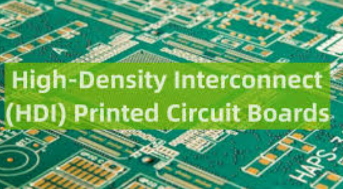
Benefits Of Ultra HDI PCB In Modern Electronics
Ultra High-Density Interconnect (HDI) Printed Circuit Boards (PCBs) have become a cornerstone in the advancement of modern electronics, offering a multitude of benefits that cater to the ever-evolving demands of the industry. As electronic devices continue to shrink in size while increasing in functionality, the need for more sophisticated and compact circuit boards has never been more critical. Ultra HDI PCBs address this need by providing a platform that supports higher component density, improved performance, and enhanced reliability.
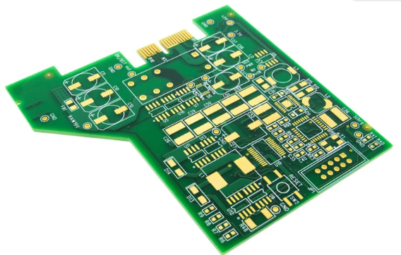
One of the primary benefits of Ultra HDI PCBs is their ability to accommodate a higher density of components.
This is achieved through the use of finer lines and spaces, smaller vias, and more precise drilling techniques. As a result, designers can place more components on a single board, which is particularly advantageous for applications where space is at a premium, such as in smartphones, tablets, and wearable devices. The increased component density not only allows for more complex circuitry but also contributes to the miniaturization of electronic devices, making them more portable and user-friendly.
In addition to supporting higher component density, Ultra HDI PCBs also offer improved electrical performance.
The shorter interconnects and reduced signal paths inherent in these boards lead to lower signal loss and reduced electromagnetic interference (EMI). This is particularly important in high-frequency applications, where signal integrity is paramount. By minimizing signal degradation, Ultra HDI PCBs ensure that electronic devices operate more efficiently and reliably, which is crucial for applications ranging from telecommunications to medical devices.
Another significant advantage of Ultra HDI PCBs is their enhanced thermal management capabilities.
As electronic devices become more powerful, they generate more heat, which can adversely affect performance and longevity. Ultra HDI PCBs are designed to dissipate heat more effectively, thanks to their advanced materials and construction techniques. This improved thermal management helps to maintain optimal operating temperatures, thereby extending the lifespan of electronic components and reducing the risk of failure.
Furthermore, Ultra HDI PCBs contribute to the overall reliability of electronic devices.
The use of advanced manufacturing processes, such as laser drilling and sequential lamination, ensures that these boards are built to exacting standards. This results in fewer defects and higher yields, which translates to more reliable end products. Additionally, the robust construction of Ultra HDI PCBs makes them more resistant to mechanical stress and environmental factors, further enhancing their durability and dependability.
The benefits of Ultra HDI PCBs are not limited to performance and reliability; they also offer significant cost advantages.
While the initial investment in Ultra HDI technology may be higher, the long-term savings can be substantial. The increased component density and improved performance of these boards can lead to reduced material costs, lower assembly costs, and fewer required layers in multilayer PCBs. Moreover, the enhanced reliability and longevity of Ultra HDI PCBs can result in lower maintenance and replacement costs over the lifecycle of the electronic device.
In conclusion, Ultra HDI PCBs represent a significant advancement in the field of electronics, offering numerous benefits that address the challenges of modern device design. By enabling higher component density, improved electrical performance, enhanced thermal management, and greater reliability, these advanced circuit boards are instrumental in the development of smaller, more powerful, and more dependable electronic devices. As the demand for cutting-edge technology continues to grow, the role of Ultra HDI PCBs in shaping the future of electronics cannot be overstated.
Challenges And Solutions In Ultra HDI PCB Design
The design of Ultra High-Density Interconnect (Ultra HDI) printed circuit boards (PCBs) presents a unique set of challenges that require innovative solutions to overcome. As electronic devices continue to shrink in size while increasing in functionality, the demand for Ultra HDI PCBs has surged.
These advanced PCBs are characterized by their extremely fine lines and spaces, high layer counts, and microvias, which enable the integration of more components in a smaller area. However, the complexity of designing such intricate boards introduces several technical and manufacturing hurdles.
One of the primary challenges in Ultra HDI PCB design is maintaining signal integrity.
As the density of the interconnects increases, the risk of signal interference and crosstalk also rises. This can lead to degraded performance and reliability issues in the final product. To mitigate these problems, designers must employ advanced simulation tools to model and predict signal behavior. Additionally, careful consideration of trace routing, impedance control, and the use of differential pairs can help maintain signal integrity. Implementing these strategies requires a deep understanding of electromagnetic theory and the specific requirements of the application.
Another significant challenge is the thermal management of Ultra HDI PCBs.
The high component density and increased power consumption can lead to excessive heat generation, which, if not properly managed, can cause component failure and reduce the lifespan of the device. Effective thermal management solutions include the use of thermal vias, heat sinks, and advanced materials with high thermal conductivity. Moreover, designers must consider the placement of heat-generating components and ensure adequate airflow within the device. Thermal simulation software can be invaluable in predicting and addressing potential thermal issues during the design phase.
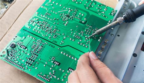
Manufacturing Ultra HDI PCBs also presents its own set of challenges.
The fine lines and spaces required for these boards demand high-precision fabrication techniques. Traditional photolithography processes may not be sufficient, necessitating the use of advanced methods such as laser direct imaging (LDI) and semi-additive processes (SAP). These techniques allow for the creation of finer features with greater accuracy. However, they also require specialized equipment and expertise, which can increase production costs and lead times. Collaboration between designers and manufacturers is crucial to ensure that the design can be reliably produced within the desired specifications.
Furthermore, the inspection and testing of Ultra HDI PCBs are more complex due to their intricate nature.
Traditional inspection methods may not be able to detect all potential defects, necessitating the use of advanced techniques such as automated optical inspection (AOI) and X-ray inspection. These methods can identify issues such as misaligned vias, insufficient solder joints, and other defects that could compromise the board’s performance. Implementing rigorous testing protocols is essential to ensure the reliability and functionality of the final product.
In conclusion, the design and manufacture of Ultra HDI PCBs involve a multitude of challenges that require innovative solutions and a collaborative approach. Maintaining signal integrity, managing thermal issues, employing advanced fabrication techniques, and implementing thorough inspection and testing protocols are all critical to the successful development of these advanced PCBs. As technology continues to evolve, ongoing research and development will be essential to address these challenges and push the boundaries of what is possible in Ultra HDI PCB design.
Future Trends In Ultra HDI PCB Technology
The landscape of printed circuit board (PCB) technology is continually evolving, and one of the most significant advancements in recent years is the development of Ultra High-Density Interconnect (Ultra HDI) PCBs. As electronic devices become increasingly compact and complex, the demand for PCBs that can support higher component densities and finer lines and spaces has surged. Ultra HDI PCBs are at the forefront of this technological evolution, offering unprecedented capabilities that are poised to shape the future of electronics manufacturing.
One of the primary trends in Ultra HDI PCB technology is the ongoing miniaturization of electronic components.
As consumer electronics, such as smartphones, wearables, and IoT devices, continue to shrink in size, the need for PCBs that can accommodate smaller and more densely packed components becomes critical. Ultra HDI PCBs, with their ability to support microvias, fine lines, and spaces, are ideally suited to meet this demand. This trend is expected to accelerate as manufacturers strive to create even more compact and powerful devices.
In addition to miniaturization, the increasing complexity of electronic devices is driving the need for more advanced PCB technologies.
Modern devices often require multiple layers of interconnections to support their sophisticated functionalities. Ultra HDI PCBs, with their multi-layer capabilities, enable the integration of complex circuits within a compact footprint. This is particularly important in applications such as advanced driver-assistance systems (ADAS) in automotive electronics, where high performance and reliability are paramount.
Another significant trend in Ultra HDI PCB technology is the push towards higher data transfer rates.
As the demand for faster and more efficient data processing continues to grow, PCBs must be capable of supporting high-speed signal transmission. Ultra HDI PCBs, with their fine lines and spaces, reduce signal loss and crosstalk, thereby enhancing signal integrity. This makes them ideal for applications in telecommunications, data centers, and high-performance computing, where high-speed data transfer is essential.
The adoption of advanced materials is also playing a crucial role in the evolution of Ultra HDI PCBs.
Traditional PCB materials, such as FR-4, are being supplemented or replaced by high-performance materials that offer better thermal and electrical properties. These advanced materials enable Ultra HDI PCBs to operate reliably in demanding environments, such as aerospace and defense applications, where extreme temperatures and harsh conditions are common. The use of advanced materials also contributes to the overall miniaturization and performance enhancement of electronic devices.
Furthermore, the integration of advanced manufacturing techniques is revolutionizing the production of Ultra HDI PCBs.
Techniques such as laser drilling, additive manufacturing, and advanced photolithography are enabling the creation of finer features and more precise interconnections. These manufacturing advancements not only improve the performance and reliability of Ultra HDI PCBs but also reduce production costs and lead times. As these techniques continue to mature, they are expected to become more widely adopted, further driving the growth of Ultra HDI PCB technology.
In conclusion, the future of Ultra HDI PCB technology is characterized by several key trends, including miniaturization, increased complexity, higher data transfer rates, advanced materials, and innovative manufacturing techniques. These trends are collectively driving the development of more compact, powerful, and reliable electronic devices. As the demand for advanced electronics continues to rise, Ultra HDI PCBs will play an increasingly vital role in meeting the technological challenges of the future. The ongoing advancements in this field promise to unlock new possibilities and set new standards in the world of electronics manufacturing.