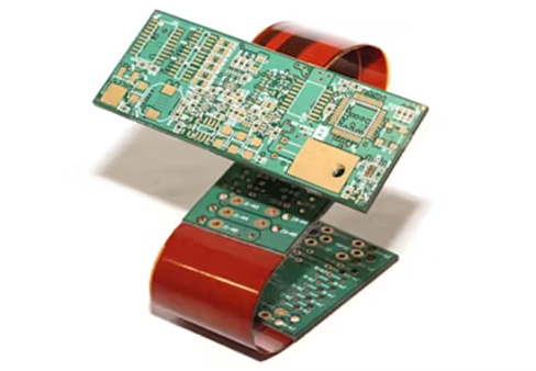
Ultra thin flex pcb
Advantages Of Ultra Thin Flex PCB In Modern Electronics
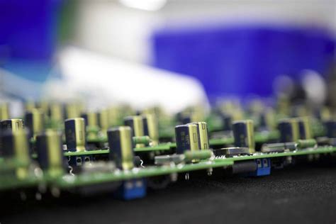
Ultra thin flexible printed circuit boards (PCBs) have emerged as a transformative technology in the realm of modern electronics, offering a multitude of advantages that cater to the evolving demands of contemporary devices. These advanced PCBs are characterized by their remarkable thinness and flexibility, which enable them to be integrated into a wide array of applications, from consumer electronics to medical devices and beyond.
One of the primary benefits of ultra thin flex PCBs is their ability to conform to complex shapes and contours,
which is particularly advantageous in the design of compact and lightweight electronic devices. This flexibility allows for innovative product designs that were previously unattainable with traditional rigid PCBs.
In addition to their adaptability, ultra thin flex PCBs contribute significantly to the miniaturization of electronic devices.
As consumer preferences shift towards smaller, more portable gadgets, the demand for components that can fit into limited spaces without compromising functionality has surged. Ultra thin flex PCBs meet this demand by providing a solution that not only saves space but also reduces the overall weight of the device. This is especially critical in applications such as wearable technology, where comfort and ease of use are paramount.
Moreover, the reliability and durability of ultra thin flex PCBs are noteworthy.
These PCBs are designed to withstand mechanical stress and environmental factors, making them ideal for use in harsh conditions. For instance, in the automotive industry, where electronic components are exposed to extreme temperatures and vibrations, ultra thin flex PCBs offer a robust solution that ensures consistent performance. Similarly, in medical devices, where precision and reliability are crucial, these PCBs provide the necessary resilience to maintain functionality over extended periods.
Another significant advantage of ultra thin flex PCBs is their potential for cost savings in both manufacturing and assembly processes.
The inherent flexibility of these PCBs allows for more efficient use of materials, reducing waste and lowering production costs. Additionally, their ability to integrate multiple functions into a single, compact unit simplifies the assembly process, leading to reduced labor costs and shorter production times. This efficiency is particularly beneficial in high-volume manufacturing environments, where time and cost savings can have a substantial impact on overall profitability.
Furthermore, the electrical performance of ultra thin flex PCBs is exceptional.
These PCBs offer excellent signal integrity and reduced electromagnetic interference (EMI), which are critical factors in the performance of high-speed electronic devices. The thin and flexible nature of these PCBs allows for shorter signal paths and improved electrical connections, resulting in faster and more reliable data transmission. This is particularly important in applications such as telecommunications and data centers, where high-speed data transfer is essential.
In conclusion, the advantages of ultra thin flex PCBs in modern electronics are manifold.
Their flexibility, adaptability, and ability to contribute to the miniaturization of devices make them an invaluable component in the design and manufacture of contemporary electronic products. The reliability, durability, and cost-saving potential further enhance their appeal, while their superior electrical performance ensures that they meet the stringent demands of high-speed applications. As technology continues to advance, the role of ultra thin flex PCBs in shaping the future of electronics is poised to become even more significant, driving innovation and enabling the development of next-generation devices.
Manufacturing Techniques For Ultra Thin Flex PCB
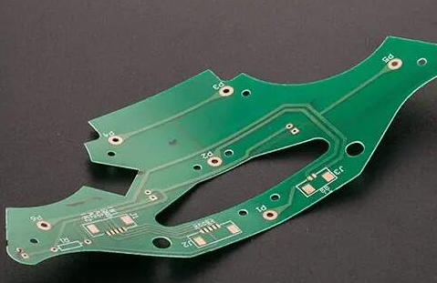
The manufacturing of ultra-thin flexible printed circuit boards (PCBs) involves a series of intricate processes that demand precision and advanced technology. These PCBs, characterized by their lightweight and flexible nature, are increasingly utilized in various high-tech applications, including wearable devices, medical instruments, and compact electronic gadgets. To achieve the desired thinness and flexibility, manufacturers employ several specialized techniques that ensure both the structural integrity and functionality of the final product.
Initially, the selection of materials plays a crucial role in the manufacturing process.
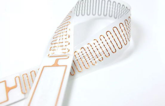
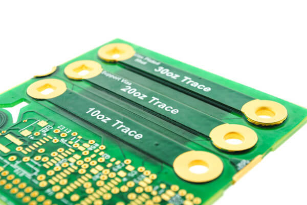
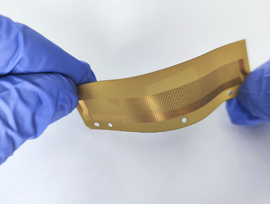
Polyimide films are commonly chosen due to their excellent thermal stability, mechanical strength, and flexibility. These films serve as the substrate upon which the circuit is built. The thickness of the polyimide film is a critical factor, typically ranging from 12.5 to 50 micrometers, depending on the specific application requirements. The choice of copper foil, which forms the conductive layer, is equally important. Ultra-thin copper foils, often less than 18 micrometers thick, are preferred to maintain the overall thinness of the PCB.
Following material selection, the next step involves the application of the copper foil onto the polyimide substrate.
This is achieved through a lamination process, where heat and pressure are applied to bond the copper foil to the substrate. The lamination process must be meticulously controlled to prevent any defects that could compromise the flexibility and performance of the PCB. Once the copper foil is securely laminated, the circuit pattern is created using photolithography. This technique involves coating the copper surface with a photoresist, exposing it to ultraviolet light through a mask that defines the circuit pattern, and then developing the exposed photoresist to reveal the underlying copper.
Subsequently, the exposed copper is etched away using a chemical solution, leaving behind the desired circuit pattern.
The etching process must be precisely controlled to ensure that the copper traces are uniform and free of defects. After etching, the remaining photoresist is stripped away, revealing the completed circuit pattern on the ultra-thin substrate. To enhance the durability and reliability of the PCB, a protective layer, such as a solder mask, is applied. This layer not only protects the copper traces from oxidation and environmental damage but also prevents solder bridges during component assembly.
In addition to these standard processes, advanced techniques such as laser drilling and precision cutting are employed to create vias and define the final shape of the PCB.
Laser drilling allows for the creation of extremely small and precise holes, which are essential for interlayer connections in multi-layer PCBs. Precision cutting, often performed using laser or mechanical methods, ensures that the PCB edges are smooth and free of burrs, which is critical for maintaining the integrity of the ultra-thin structure.
Throughout the manufacturing process, rigorous quality control measures are implemented to detect and rectify any defects.
Automated optical inspection (AOI) systems are commonly used to examine the circuit patterns for any discrepancies. Electrical testing is also conducted to verify the continuity and functionality of the circuits. These quality control steps are vital to ensure that the final product meets the stringent requirements of modern electronic applications.
In conclusion, the manufacturing of ultra-thin flexible PCBs involves a combination of material selection, precise lamination, photolithography, etching, protective coating, and advanced drilling and cutting techniques. Each step requires meticulous attention to detail and advanced technology to produce PCBs that are not only thin and flexible but also reliable and durable. As technology continues to advance, the demand for ultra-thin flex PCBs is expected to grow, driving further innovations in manufacturing techniques.

Applications Of Ultra Thin Flex PCB In Wearable Technology
Ultra thin flexible printed circuit boards (PCBs) have revolutionized the landscape of wearable technology, offering unprecedented versatility and functionality. These advanced PCBs are characterized by their remarkable thinness and flexibility, which enable them to be integrated seamlessly into a variety of wearable devices. The applications of ultra thin flex PCBs in wearable technology are vast and continually expanding, driven by the demand for more compact, lightweight, and efficient devices.
One of the primary applications of ultra thin flex PCBs in wearable technology is in the realm of fitness trackers.
These devices, which monitor physical activity and health metrics, benefit immensely from the flexibility and durability of ultra thin flex PCBs. The ability to bend and conform to the contours of the human body ensures that fitness trackers are comfortable to wear and can provide accurate readings. Moreover, the lightweight nature of these PCBs contributes to the overall comfort and wearability of the device, making it less intrusive for users during their daily activities.
In addition to fitness trackers, smartwatches are another significant application of ultra thin flex PCBs.
Smartwatches require a high degree of integration of various components, including sensors, processors, and communication modules, within a limited space. Ultra thin flex PCBs facilitate this integration by allowing for complex circuit designs that can be folded or bent to fit within the compact form factor of a smartwatch. This not only enhances the functionality of the device but also contributes to its sleek and modern design, which is a critical factor for consumer appeal.
Medical wearables represent another crucial area where ultra thin flex PCBs are making a substantial impact.
Devices such as continuous glucose monitors, heart rate monitors, and other health monitoring systems rely on the precision and reliability of their electronic components. Ultra thin flex PCBs provide the necessary flexibility to ensure that these devices can be worn comfortably for extended periods, which is essential for continuous monitoring. Furthermore, the robustness of these PCBs ensures that the devices can withstand the rigors of daily use without compromising performance.
The integration of ultra thin flex PCBs in wearable technology also extends to the realm of smart clothing.
Smart textiles, which incorporate electronic components into fabrics, are gaining traction for their potential to monitor various physiological parameters and provide real-time feedback. Ultra thin flex PCBs are ideal for this application due to their ability to be embedded within the fabric without adding significant bulk or weight. This integration allows for the creation of garments that can monitor heart rate, body temperature, and other vital signs, providing valuable data for both fitness enthusiasts and medical professionals.
Moreover, the use of ultra thin flex PCBs in wearable technology is not limited to consumer and medical applications.
Industrial and military sectors are also exploring the potential of these advanced PCBs for creating wearable devices that can enhance safety and efficiency. For instance, wearable sensors embedded in protective gear can monitor environmental conditions and provide alerts in hazardous situations, thereby improving worker safety.
In conclusion, the applications of ultra thin flex PCBs in wearable technology are diverse and continually evolving. Their unique properties of flexibility, thinness, and durability make them indispensable for the development of next-generation wearable devices. As technology advances, it is anticipated that the role of ultra thin flex PCBs will expand further, driving innovation and enhancing the capabilities of wearable technology across various domains.
Design Challenges And Solutions For Ultra Thin Flex PCB
Designing ultra-thin flexible printed circuit boards (PCBs) presents a unique set of challenges and requires innovative solutions to ensure functionality, reliability, and manufacturability. As electronic devices continue to shrink in size while increasing in complexity, the demand for ultra-thin flex PCBs has surged. These PCBs are essential in applications where space constraints and flexibility are critical, such as in wearable technology, medical devices, and advanced consumer electronics.
One of the primary challenges in designing ultra-thin flex PCBs is maintaining mechanical integrity.
Due to their reduced thickness, these PCBs are more susceptible to mechanical stress and damage. To address this, designers must carefully select materials that offer a balance between flexibility and durability. Polyimide films are commonly used due to their excellent thermal stability and mechanical properties. Additionally, incorporating protective layers, such as coverlays or solder masks, can enhance the mechanical robustness of the PCB without significantly increasing its thickness.
Another significant challenge is ensuring electrical performance.
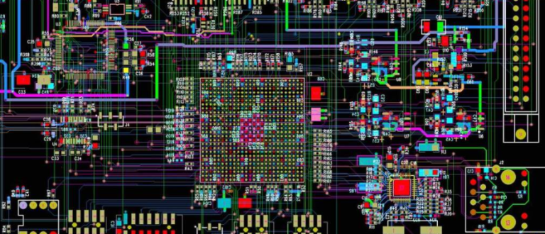
Ultra-thin flex PCBs often require fine-pitch components and high-density interconnects, which can lead to signal integrity issues such as crosstalk and electromagnetic interference (EMI). To mitigate these problems, designers can employ advanced layout techniques, such as controlled impedance routing and differential pair routing. Furthermore, the use of low-loss dielectric materials can help maintain signal integrity by reducing signal attenuation and dispersion.
Thermal management is also a critical consideration in the design of ultra-thin flex PCBs.
The reduced thickness of these PCBs can limit their ability to dissipate heat, potentially leading to overheating and reduced reliability. To overcome this, designers can incorporate thermal vias and heat spreaders to enhance heat dissipation. Additionally, selecting materials with high thermal conductivity can help manage heat more effectively. In some cases, integrating active cooling solutions, such as micro-fans or thermoelectric coolers, may be necessary to maintain optimal operating temperatures.
Manufacturability is another area where ultra-thin flex PCBs pose challenges.
The delicate nature of these PCBs requires precise handling and processing techniques to avoid damage during manufacturing. Advanced fabrication methods, such as laser drilling and precision etching, are often employed to achieve the fine features required for ultra-thin flex PCBs. Additionally, automated optical inspection (AOI) and other quality control measures are essential to ensure that the PCBs meet stringent performance and reliability standards.
Despite these challenges, several solutions have been developed to facilitate the design and manufacturing of ultra-thin flex PCBs.
For instance, advancements in material science have led to the development of new substrates and adhesives that offer improved performance characteristics. Moreover, the adoption of computer-aided design (CAD) tools and simulation software allows designers to model and optimize their PCB layouts before fabrication, reducing the risk of errors and improving overall design efficiency.
In conclusion, while the design and manufacturing of ultra-thin flex PCBs present numerous challenges, a combination of innovative materials, advanced fabrication techniques, and meticulous design practices can overcome these obstacles. As technology continues to evolve, the demand for ultra-thin flex PCBs is expected to grow, driving further advancements in this field. By addressing the mechanical, electrical, thermal, and manufacturability challenges, designers can create reliable and high-performance ultra-thin flex PCBs that meet the needs of modern electronic applications.