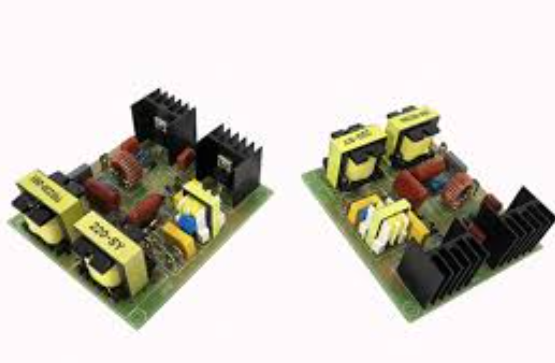
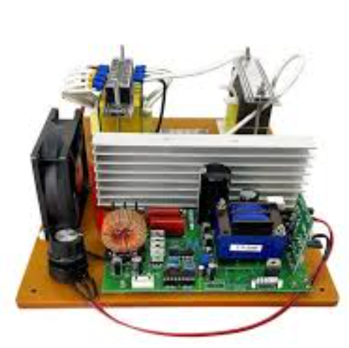
Ultrasonic pcb
Understanding The Basics Of Ultrasonic PCB Technology
Ultrasonic PCB technology represents a significant advancement in the field of electronics, offering a range of benefits that enhance the performance and reliability of printed circuit boards (PCBs). At its core, ultrasonic PCB technology involves the use of high-frequency sound waves to facilitate various processes, such as cleaning, bonding, and inspection. This innovative approach leverages the unique properties of ultrasonic waves to achieve results that are often unattainable through conventional methods.
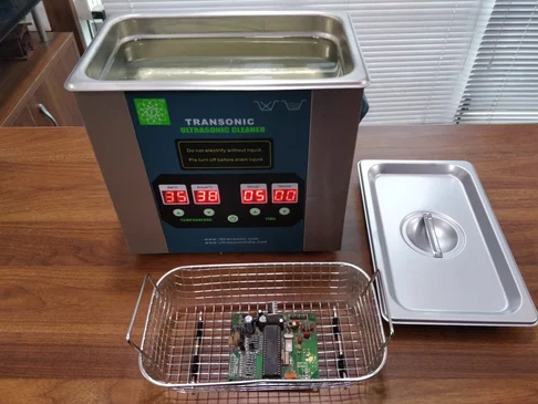
To begin with, the cleaning process in ultrasonic PCB technology is particularly noteworthy.
Traditional cleaning methods, which often rely on solvents and mechanical scrubbing, can be both time-consuming and potentially damaging to delicate components. In contrast, ultrasonic cleaning utilizes high-frequency sound waves to create microscopic cavitation bubbles in a cleaning solution. These bubbles implode upon contact with the PCB surface, effectively dislodging contaminants without causing physical harm to the components. This method ensures a thorough and gentle cleaning process, which is crucial for maintaining the integrity and functionality of the PCB.
Moving on to bonding, ultrasonic PCB technology offers a superior alternative to traditional soldering techniques.
Ultrasonic bonding employs high-frequency vibrations to generate localized heat at the interface of the materials being joined. This process, known as ultrasonic welding, creates strong and reliable bonds without the need for additional adhesives or solder. The precision and control afforded by ultrasonic welding make it particularly suitable for applications where traditional soldering might pose challenges, such as in the assembly of microelectronic components or in environments where thermal sensitivity is a concern.
Furthermore, ultrasonic inspection plays a critical role in ensuring the quality and reliability of PCBs.
This non-destructive testing method uses ultrasonic waves to detect flaws and defects within the PCB structure. By analyzing the reflections and transmissions of these waves, technicians can identify issues such as delaminations, voids, and cracks that may not be visible through other inspection techniques. The ability to detect and address these defects early in the manufacturing process helps to prevent failures and improve the overall reliability of the final product.
In addition to these specific applications, the broader implications of ultrasonic PCB technology are also worth considering.
The adoption of ultrasonic methods can lead to significant improvements in manufacturing efficiency and cost-effectiveness. For instance, the reduced need for chemical solvents in cleaning processes not only lowers material costs but also minimizes environmental impact. Similarly, the precision and reliability of ultrasonic bonding can reduce the incidence of rework and scrap, further enhancing production efficiency.
Moreover, the versatility of ultrasonic PCB technology allows it to be integrated into a wide range of applications across various industries.
From consumer electronics to aerospace and medical devices, the benefits of ultrasonic methods are being increasingly recognized and utilized. As the demand for smaller, more complex, and higher-performing electronic devices continues to grow, the role of ultrasonic PCB technology is likely to become even more prominent.
In conclusion, understanding the basics of ultrasonic PCB technology reveals its potential to revolutionize the way printed circuit boards are manufactured and maintained. By harnessing the power of high-frequency sound waves, this technology offers enhanced cleaning, bonding, and inspection capabilities that contribute to the production of more reliable and efficient electronic devices. As advancements in this field continue to unfold, the impact of ultrasonic PCB technology is poised to expand, driving further innovation and excellence in the electronics industry.
Applications Of Ultrasonic PCBs In Modern Electronics
Ultrasonic printed circuit boards (PCBs) have emerged as a pivotal technology in modern electronics, offering a multitude of applications that span various industries. These specialized PCBs leverage ultrasonic waves to perform a range of functions, from sensing and communication to material characterization and medical diagnostics. The integration of ultrasonic technology into PCBs has opened new avenues for innovation, enhancing the capabilities and performance of electronic devices.
One of the primary applications of ultrasonic PCBs is in the field of non-destructive testing (NDT).
Ultrasonic waves are employed to detect flaws and irregularities in materials without causing any damage. This is particularly valuable in industries such as aerospace, automotive, and construction, where the integrity of materials is critical. By embedding ultrasonic transducers into PCBs, engineers can create compact and efficient NDT systems that provide real-time data on material properties, ensuring safety and reliability.
In addition to NDT, ultrasonic PCBs are extensively used in medical diagnostics.
Ultrasonic imaging, commonly known as ultrasound, relies on high-frequency sound waves to create images of internal body structures. By integrating ultrasonic transducers into PCBs, medical devices can achieve higher precision and miniaturization. This advancement has led to the development of portable ultrasound machines, which are invaluable in remote and underserved areas. Furthermore, ultrasonic PCBs are instrumental in therapeutic applications, such as targeted drug delivery and physiotherapy, where precise control of ultrasonic waves is essential.
The automotive industry also benefits significantly from ultrasonic PCB technology.
Ultrasonic sensors are widely used in advanced driver-assistance systems (ADAS) to enhance vehicle safety. These sensors detect obstacles, measure distances, and assist in parking, thereby reducing the risk of accidents. By incorporating ultrasonic transducers into PCBs, manufacturers can produce compact and reliable sensors that seamlessly integrate into the vehicle’s electronic system. This integration not only improves the functionality of ADAS but also contributes to the overall efficiency and performance of modern vehicles.
Moreover, ultrasonic PCBs play a crucial role in industrial automation and robotics.
Ultrasonic sensors are employed to measure distances, detect objects, and monitor fluid levels in various industrial processes. The ability to embed these sensors into PCBs allows for the creation of sophisticated control systems that enhance the precision and efficiency of automated operations. This is particularly important in manufacturing environments where accuracy and reliability are paramount.
Another noteworthy application of ultrasonic PCBs is in the field of communication.
Ultrasonic waves can be used for wireless data transmission, offering an alternative to traditional radio frequency (RF) communication. This is especially useful in environments where RF signals are prone to interference or where secure communication is required. By integrating ultrasonic transducers into PCBs, engineers can develop communication systems that are both secure and efficient, catering to the needs of specialized applications.
Furthermore, ultrasonic PCBs are instrumental in environmental monitoring.
Ultrasonic sensors can detect changes in air quality, water levels, and other environmental parameters. By embedding these sensors into PCBs, researchers and environmentalists can create compact and robust monitoring systems that provide real-time data on environmental conditions. This information is crucial for making informed decisions and implementing effective measures to protect the environment.
In conclusion, the applications of ultrasonic PCBs in modern electronics are vast and varied, spanning multiple industries and contributing to advancements in technology and innovation. From non-destructive testing and medical diagnostics to automotive safety and industrial automation, ultrasonic PCBs offer unparalleled precision, efficiency, and reliability. As technology continues to evolve, the integration of ultrasonic waves into PCBs will undoubtedly play a pivotal role in shaping the future of electronics.
Design Considerations For Ultrasonic PCBs
When designing ultrasonic printed circuit boards (PCBs), several critical considerations must be taken into account to ensure optimal performance and reliability. Ultrasonic PCBs are specialized circuits used in applications such as medical imaging, industrial non-destructive testing, and distance measurement. These applications demand high precision and reliability, making the design process particularly intricate.
To begin with, the choice of materials is paramount.
The substrate material must possess excellent dielectric properties to minimize signal loss and ensure efficient transmission of ultrasonic waves. Commonly used materials include FR-4, Rogers, and ceramic substrates, each offering distinct advantages. For instance, ceramic substrates provide superior thermal stability and low dielectric loss, making them ideal for high-frequency applications. However, they are more expensive compared to FR-4, which is widely used due to its cost-effectiveness and adequate performance for many applications.
Another crucial aspect is the layout of the PCB
The layout must be meticulously planned to minimize electromagnetic interference (EMI) and crosstalk between traces. This involves careful routing of signal paths, maintaining adequate spacing between traces, and using ground planes to shield sensitive components. Additionally, the placement of components is critical; for example, placing the ultrasonic transducer close to the edge of the PCB can reduce signal attenuation and improve performance.
Thermal management is another vital consideration in the design of ultrasonic PCBs.
Ultrasonic transducers and associated circuitry can generate significant heat during operation, which can affect performance and reliability. Effective thermal management strategies include the use of thermal vias, heat sinks, and proper ventilation to dissipate heat away from critical components. Moreover, selecting components with low power consumption can help mitigate thermal issues.
Signal integrity is a key factor in ultrasonic PCB design.
High-frequency signals are susceptible to degradation due to factors such as impedance mismatches, signal reflections, and attenuation. To address these issues, designers must ensure that the impedance of transmission lines is matched to the source and load impedances. This can be achieved through careful selection of trace widths, spacing, and the use of controlled impedance techniques. Additionally, the use of differential signaling can help reduce noise and improve signal integrity.
Power supply design is also critical in ultrasonic PCBs.
Stable and noise-free power supplies are essential to ensure the proper functioning of ultrasonic transducers and associated circuitry. This involves the use of low-noise voltage regulators, proper decoupling, and filtering techniques to minimize power supply noise. Furthermore, the power distribution network must be designed to provide adequate current to all components without causing voltage drops or introducing noise.
Testing and validation are integral parts of the design process.
Prototyping and testing the PCB under real-world conditions can help identify and rectify potential issues before mass production. This includes testing for signal integrity, thermal performance, and overall functionality. Additionally, simulation tools can be used during the design phase to predict the behavior of the PCB and optimize the design accordingly.
In conclusion, designing ultrasonic PCBs requires a comprehensive understanding of material properties, layout techniques, thermal management, signal integrity, power supply design, and thorough testing. By carefully considering these factors, designers can create ultrasonic PCBs that meet the stringent requirements of high-precision applications, ensuring reliable and efficient performance.
Future Trends In Ultrasonic PCB Development
The field of ultrasonic printed circuit boards (PCBs) is poised for significant advancements, driven by the rapid evolution of technology and the increasing demand for more efficient and compact electronic devices. As we look to the future, several trends are emerging that promise to shape the development of ultrasonic PCBs, enhancing their functionality and broadening their applications.
One of the most notable trends is the miniaturization of components.
As electronic devices become smaller and more powerful, there is a growing need for PCBs that can accommodate these compact designs without compromising performance. Ultrasonic technology, with its ability to precisely manipulate materials at a microscopic level, is ideally suited to meet this demand. By enabling the creation of smaller, more intricate circuit patterns, ultrasonic PCBs can support the development of next-generation devices that are both highly functional and space-efficient.
In addition to miniaturization, there is a strong focus on improving the durability and reliability of ultrasonic PCBs.
This is particularly important in industries such as aerospace, automotive, and medical devices, where electronic components must withstand harsh environments and rigorous use. Advances in materials science are playing a crucial role in this area, with the development of new substrates and coatings that enhance the resilience of PCBs. For instance, the use of advanced polymers and composite materials can provide better resistance to thermal and mechanical stress, thereby extending the lifespan of the circuit boards.
Another key trend is the integration of smart technologies into ultrasonic PCBs.
The rise of the Internet of Things (IoT) and the increasing prevalence of connected devices are driving the need for PCBs that can support advanced functionalities such as real-time data processing, wireless communication, and energy harvesting. Ultrasonic technology can facilitate the incorporation of these features by enabling the precise placement of sensors, antennas, and other components. This integration not only enhances the capabilities of the devices but also opens up new possibilities for innovation in various sectors.
Sustainability is also becoming a critical consideration in the development of ultrasonic PCBs.
As environmental concerns continue to grow, there is a push towards more eco-friendly manufacturing processes and materials. Ultrasonic technology offers several advantages in this regard, including reduced energy consumption and lower waste generation compared to traditional methods. Moreover, the ability to use biodegradable or recyclable materials in PCB production can further minimize the environmental impact, aligning with the broader goals of sustainable development.
Furthermore, advancements in automation and artificial intelligence (AI) are set to revolutionize the production of ultrasonic PCBs.
Automated manufacturing processes can significantly increase efficiency and consistency, reducing the likelihood of defects and improving overall quality. AI-driven design tools can also optimize the layout and functionality of PCBs, ensuring that they meet the specific requirements of each application. These technologies not only streamline production but also enable more complex and customized designs, catering to the diverse needs of modern electronic devices.
In conclusion, the future of ultrasonic PCB development is characterized by several promising trends, including miniaturization, enhanced durability, smart integration, sustainability, and advanced manufacturing techniques. As these trends continue to evolve, they will undoubtedly lead to the creation of more sophisticated and versatile PCBs, driving innovation across a wide range of industries. The ongoing advancements in ultrasonic technology will play a pivotal role in this progress, paving the way for a new era of electronic design and manufacturing.


