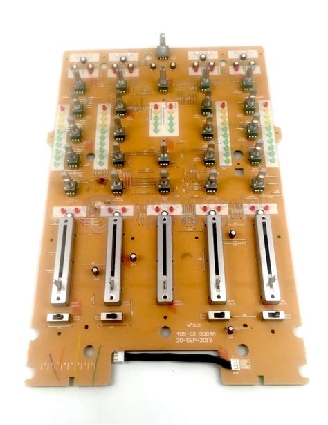
Understanding Assy PCBs: Insights into Assembly and Functionality
Key Takeaways
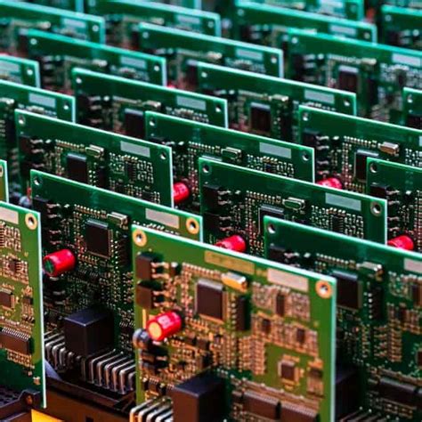
Understanding the complexities of Assy PCBs is essential for anyone involved in the creation of modern electronic devices. These Printed Circuit Board Assemblies (PCBA) serve as the backbone of electronic systems, seamlessly integrating various components to ensure optimal functionality. One of the crucial elements to consider during pcb assembly is the distinction between different assembly techniques—such as through-hole and surface mount technology—which can significantly impact both performance and cost.
It’s important to note that effective Assy PCB designs not only enhance connectivity but also improve thermal management and electromagnetic compatibility, features that are increasingly vital in today’s technology landscape. When selecting materials for pcb assembly, engineers must prioritize reliability and durability to withstand the rigors of use.
| Key Considerations in PCB Assembly | Implications |
|---|---|
| Material Choice | Affects durability, performance |
| Assembly Method | Determines cost, complexity |
| Testing Procedures | Ensures reliability |
“The right assembly process can transform an average circuit board into a reliable piece of electronic equipment.”
This nuanced understanding is fundamental not just for engineers but also for hobbyists who aspire to innovate within this space. As we progress further into an era where electronics are pivotal, grasping these core concepts will empower stakeholders to construct more effective electronic solutions.
Introduction to Assy PCBs: A Comprehensive Overview
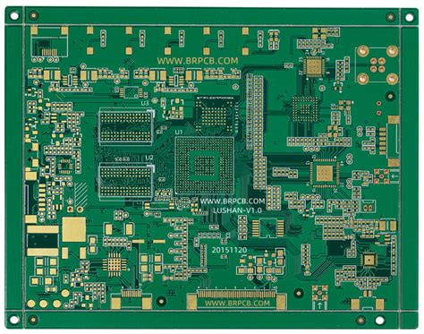
In today’s rapidly evolving technological landscape, Assy PCBs play a crucial role in the design and functionality of electronic devices. The term “pcb assembly” encompasses a range of processes involved in creating printed circuit boards that serve as the backbone for various electronic systems. Through the integration of components onto a printed circuit board assembly (PCBA), engineers can achieve higher levels of performance and reliability. Understanding these assemblies is essential for both industry professionals and electronics enthusiasts.
The design and manufacturing of Assy PCBs require meticulous attention to detail, as they are responsible for connecting different electronic components in an efficient layout. The assembly process involves multiple steps, including soldering, component placement, and inspection to ensure that the final product meets stringent quality standards. Moreover, advanced techniques such as surface mount technology (SMT) have revolutionized the way pcbs are manufactured, allowing for more compact designs with enhanced functionality.
Furthermore, the significance of Assy PCBs goes beyond mere assembly; they are integral components that determine the overall performance characteristics of modern electronics. Factors like thermal management, electrical conductivity, and signal integrity are all influenced by the quality of pcb assembly. As technology continues to advance—enabling trends such as miniaturization and greater functionality—understanding how these assemblies operate is vital for anyone involved in electronics design or manufacturing.
By delving into the intricacies of Assy PCBs, this article aims to provide valuable insights into their assembly processes and functionalities, thereby highlighting their importance in today’s high-tech world.
The Assembly Process of Assy PCBs: Steps and Techniques
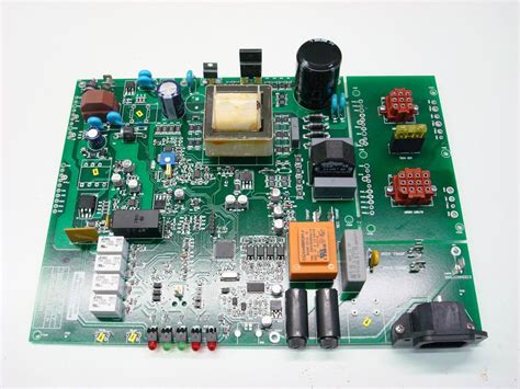
The assembly process of Assy PCBs (Printed Circuit Board Assemblies) is a critical component in ensuring the functionality and reliability of electronic devices. The journey begins with the preparation of pcb assembly components, which involves selecting the right materials and ensuring they meet the required specifications. Quality control is paramount; therefore, each component must be inspected before being placed on the board. Once components are prepared, they undergo a meticulous placement process, where both automated machinery and skilled technicians work collaboratively to position components accurately onto the printed circuit boards.
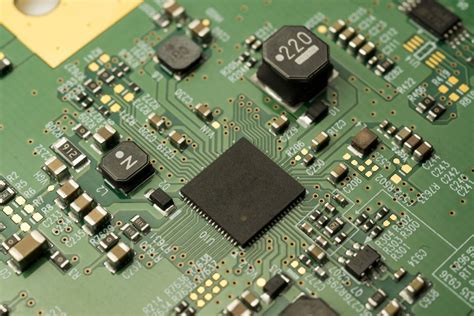
Following component placement, soldering techniques play an essential role in securing these components. Both surface mount technology (SMT) and through-hole methods are commonly utilized in this stage to achieve reliable connections. The use of PCBA techniques greatly enhances the effectiveness of soldering operations, ensuring durability and conductivity. After soldering, boards typically go through reflow or wave soldering processes, which finalize connections through precise heating systems tailored to melt solder without damaging sensitive components.
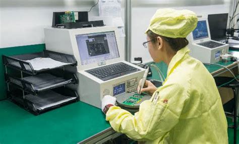
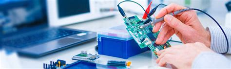
Once assembled, each board must undergo a thorough testing phase to ensure functionality. This may include electrical testing, visual inspections, and sometimes functional tests that simulate end-user scenarios. Addressing common challenges such as alignment issues or solder defects during this stage is critical to optimizing yield rates in pcb assembly operations. By effectively managing these steps and techniques within the assembly process, engineers can significantly enhance both the performance and longevity of Assy PCBs, thus contributing positively to modern electronics.
Key Functionalities of Assy PCBs in Modern Electronics
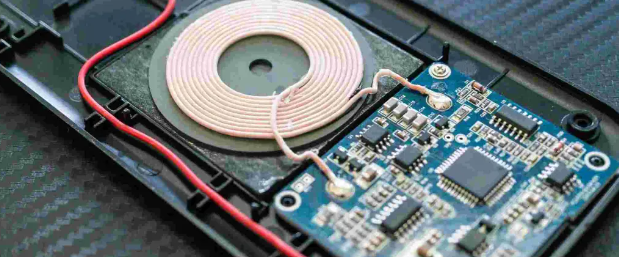
Assy PCBs, or printed circuit board assemblies, play a crucial role in the functionality of modern electronic devices. Their design and execution facilitate the interconnection of various electronic components, which is essential for proper device operation. One of the primary functionalities of Assy PCBs is to serve as a platform for mounting electronic components—be it resistors, capacitors, or integrated circuits—allowing for efficient space management while ensuring robust electrical connections. Additionally, through advanced techniques in pcb assembly, these assemblies enable streamlined power distribution and signal transmission, which are critical for high-performance applications.
Another key aspect is the versatility provided by pcba in supporting different technologies and configurations. Whether it’s through surface mount technology (SMT) or through-hole mounting, Assy PCBs can accommodate various designs tailored for specific applications, such as consumer electronics, automotive systems, or industrial equipment. This adaptability ensures that products can meet evolving industry standards while maximizing efficiency and reliability. Furthermore, with the growing emphasis on miniaturization in electronics, the compact design inherent in Assy PCBs supports emerging technologies by facilitating smaller devices without sacrificing performance. The integration of thermal management solutions within these assemblies also enhances operational stability under diverse environmental conditions.
Thus, understanding the key functionalities of Assy PCBs empowers engineers and designers to create more efficient and effective electronic systems that meet today’s technological demands.
Importance of Assy PCBs in the Electronics Industry
The significance of Assy PCBs (Printed Circuit Board Assemblies) in the electronics industry cannot be overstated. These components serve as the backbone for a wide array of electronic devices, ensuring functionality and reliability. The intricate process of pcb assembly integrates various electronic parts into a cohesive unit, enabling their effective operation in devices ranging from simple gadgets to complex machinery. The transition from raw components to a finished PCBA not only highlights the importance of precision in design but also emphasizes quality control at every stage of assembly. As technology continues to evolve at an unprecedented pace, the role of Assy PCBs becomes increasingly crucial. They are pivotal in facilitating advancements such as miniaturization, cost reduction, and improved performance across multiple sectors including consumer electronics, automotive applications, and industrial automation. Understanding the dynamics involved in pcb assembly stages helps engineers and manufacturers mitigate risks and optimize functionality while meeting strict industry standards. Ultimately, the importance of Assy PCBs lies not just in their assembly but also in their ability to adapt to new technologies and innovations, solidifying their place at the forefront of modern electronics development.
Common Challenges in Assy PCB Assembly and Solutions
The process of pcb assembly presents several challenges that engineers and technicians must navigate to ensure the successful production of PCBA (Printed Circuit Board Assembly). One of the most prevalent issues is related to component placement accuracy. Misaligned components can lead to failures in functionality and ultimately affect the performance of the entire assembly. To address this, utilizing advanced pick-and-place machines with high precision and conducting thorough inspections during the assembly process are essential strategies. Another challenge involves soldering defects, such as cold solder joints or bridging, which can compromise electrical connectivity. Implementing controlled soldering techniques and optimizing reflow profiles can significantly reduce these issues. Additionally, managing thermal profiles during assembly is crucial, as excessive heat can damage sensitive components. Employing precise thermal management systems during the pcb assembly process ensures that each component receives an optimal level of heat without exceeding its threshold. Overall, by recognizing these common challenges in Assy PCB assembly and applying effective solutions, manufacturers can enhance quality control while reducing production costs and lead times, ultimately supporting the electronics industry’s demand for reliable products.
Innovations in Assy PCB Technology: Trends and Future Directions
The landscape of Assy PCBs is continually evolving, driven by the rapid advancements in technology and increasing demands for efficiency and performance in electronic devices. One of the key trends shaping the future of pcb assembly is the integration of automation and robotics into the PCBA processes. This shift not only enhances the precision of manufacturing but also significantly reduces production times, ultimately leading to lower costs for both manufacturers and consumers. Moreover, as the complexity of electronic designs increases, innovative materials are being developed for Assy PCBs that offer improved thermal management and greater durability. For instance, the adoption of flexible printed circuit boards (FPCBs) allows for more compact designs while maintaining functionality, which is crucial for modern applications such as wearable technology and IoT devices. Additionally, industries are increasingly focusing on sustainability; thus, eco-friendly materials are gaining traction in pcb assembly, influencing both production methods and final product designs. The incorporation of advanced simulation tools during the design phase is also proving to be transformative, enabling engineers to foresee potential issues and optimize performance before physical prototypes are produced. As these innovations continue to unfold, they promise not only to redefine efficiency but also to expand the horizons of what is possible within electronic design and functionality.
Best Practices for Engineers: Working with Assy PCBs
When engaging in pcb assembly processes, engineers must adhere to a series of best practices that enhance not only the quality of the assembly but also the efficiency of production. A crucial aspect is ensuring that all components meet the required specifications before they enter the assembly line. Verifying component compatibility minimizes issues related to mal-functioning or performance, which could arise from incompatible parts. During pcba execution, it is essential to maintain a clean and organized workspace; this helps prevent contamination and reduces the potential for errors.
Additionally, engineers should invest time in thorough training for technicians involved in Assy PCB processes. Developing an understanding of techniques such as soldering, surface mount technology, and inspection methods will significantly improve overall outcomes. Utilizing advanced software tools for design verification can streamline the process, allowing engineers to simulate and assess potential issues before physical assembly occurs. Regular maintenance of machinery and equipment is also vital; ensuring that tools are calibrated correctly can prevent defects during the pcb assembly process.
Finally, engineers should encourage collaboration among team members since shared knowledge can lead to discovering innovative solutions for common challenges encountered in pcba tasks. By fostering a culture of communication and continuous improvement, teams can significantly enhance their workflow and output quality when working with Assy PCBs.
Conclusion: The Vital Role of Assy PCBs in Electronic Design
In summarizing the significance of Assy PCBs, it is essential to recognize their pivotal role in the realm of electronic design. The process of pcb assembly is not merely a collection of steps but a sophisticated interplay of technology and craftsmanship. Each PCBA (Printed Circuit Board Assembly) serves as the backbone of numerous electronic devices, ensuring that electrical components are not only securely connected but also optimally functioning. The intricate design and assembly procedures underscore the importance of precision, as even minor deviations can result in system failures or inefficient performance. Furthermore, with the rapid advancement in electronic technology, the demand for innovative Assy PCBs is only set to rise. Engineers must stay abreast of emerging trends and best practices to harness the full potential of these assemblies. Emphasizing quality during pcb assembly guarantees durability and reliability, which are paramount in today’s fast-paced electronics industry. The cumulative knowledge surrounding PCBA technologies empowers both engineers and enthusiasts, highlighting that mastering these techniques is crucial for future advancements in electronic design and functionality.
Conclusion: The Vital Role of Assy PCBs in Electronic Design
In summary, Assy PCBs play a crucial role in the field of electronic design, effectively bridging the gap between raw electronic components and functional devices. The pcb assembly process serves as the backbone of modern electronics, ensuring that components are strategically placed and connected to create reliable and efficient products. Through meticulous pcba processes, designers can achieve optimal performance and functionality in their devices. Recognizing the importance of these assemblies allows engineers to appreciate how each layer of assembly contributes to the overall effectiveness of electronic systems. As technologies continue to advance, understanding the nuances of Assy PCBs will be essential for professionals striving to innovate and maintain competitiveness in a fast-evolving industry. The commitment to excellence in pcb assembly reflects not only in product performance but also enhances user satisfaction and trust in technological advancements. Therefore, prioritizing quality and efficiency in pcba will remain a pivotal focus for engineers and manufacturers alike as they navigate the complexities of modern electronics.
FAQs
What is an Assy PCB?
An Assy PCB, or Assembly Printed Circuit Board, is a completed assembly where all electronic components are integrated onto the PCB. This assembly process is crucial for the functionality of electronic devices.
What is the importance of PCB assembly in electronics?
PCB assembly, commonly referred to as PCBA, plays a vital role in modern electronics. It ensures that all components are correctly soldered and positioned on the PCB, allowing devices to function efficiently and reliably.
What are the common techniques used in PCB assembly?
Common techniques include surface mount technology (SMT) and through-hole technology (THT). These methods cater to various specifications in pcb assembly, balancing size, performance, and cost.
How do I troubleshoot issues in PCBA?
Troubleshooting PCBA issues often involves inspecting solder joints, measuring component values, and confirming that connections align with design specifications. Understanding these aspects is critical in maintaining quality during pcb assembly.
What advancements are influencing Assy PCB technology today?
Innovations such as automated assembly processes, improved soldering materials, and advancements in design software significantly enhance the efficiency and effectiveness of pcb assembly, driving progress in the electronics sector.