Understanding Creepage Distance in PCB Design
Introduction to Creepage Distance
In printed circuit board (PCB) design, creepage distance represents a critical safety parameter that determines the shortest path between two conductive parts along the surface of the insulating material. This concept plays a fundamental role in ensuring electrical safety and preventing potential failures in electronic devices.
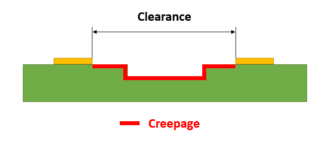
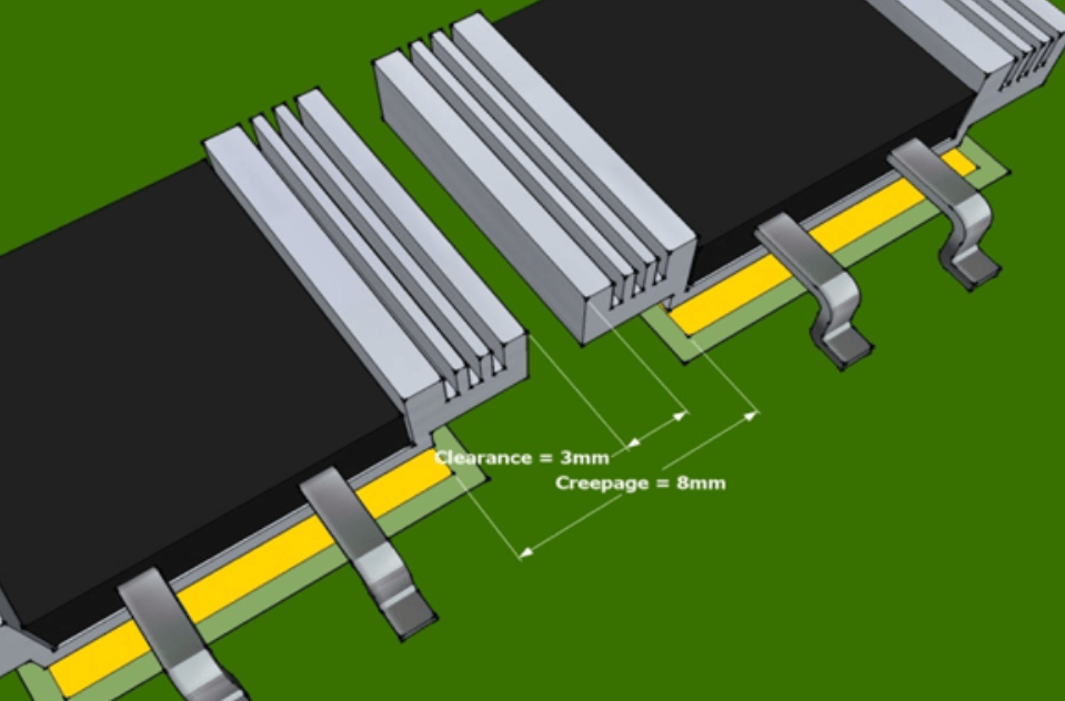
Creepage distance differs from clearance (the straight-line distance through air between conductors) as it specifically measures the surface path that electrical current might travel across insulating materials. Proper understanding and implementation of creepage distance requirements help prevent several failure modes including:
- Electrical arcing across surfaces
- Tracking (formation of conductive paths along insulation surfaces)
- Corrosion-induced failures
- Long-term insulation breakdown
For PCB designers, mastering creepage distance principles is essential for creating reliable, safe, and compliant electronic products that meet international safety standards.
Fundamental Concepts and Definitions
Clearance vs. Creepage: Key Differences
While often confused, clearance and creepage represent distinct concepts in PCB safety:
Clearance: The shortest distance through air between two conductive parts. This measures the straight-line separation that would prevent arcing through air.
Creepage: The shortest path along the surface of an insulating material between two conductive parts. This accounts for possible surface contamination or degradation that could create conductive paths.
The critical distinction lies in the medium considered – clearance deals with air gaps while creepage considers surface paths across solid insulation.
Tracking and Its Relationship to Creepage
Tracking describes the phenomenon where insulation surfaces develop conductive paths due to:
- Electrolytic contamination (dust, moisture, etc.)
- Electrical stress over time
- Surface degradation from small electrical discharges
Creepage distance requirements aim to prevent tracking by ensuring sufficient separation between conductors, even when surface contamination occurs.
Comparative Tracking Index (CTI)
The CTI measures an insulating material’s resistance to tracking, expressed as the voltage that causes tracking after 50 drops of contaminant solution. Materials are classified into CTI groups:
- CTI ≥ 600: Group I (best tracking resistance)
- 400 ≤ CTI < 600: Group II
- 175 ≤ CTI < 400: Group IIIa
- 100 ≤ CTI < 175: Group IIIb (poorest tracking resistance)
Higher CTI values allow for reduced creepage distances as the material inherently resists tracking better.
Factors Affecting Creepage Distance Requirements
Voltage Considerations
The working voltage and transient overvoltages primarily determine required creepage distances. Higher voltages necessitate greater separation. Key voltage-related factors include:
- RMS or DC working voltage: The normal operating voltage
- Peak working voltage: Important for non-sinusoidal waveforms
- Transient overvoltages: Short-duration voltage spikes
- Pollution degree: Environmental contamination affects requirements
Environmental Conditions
Environmental factors significantly influence creepage distance needs:
- Pollution Degrees:
- Pollution Degree 1: Clean environments (sealed enclosures)
- Pollution Degree 2: Normally dry, non-conductive pollution
- Pollution Degree 3: Conductive pollution or dry non-conductive pollution becoming conductive temporarily
- Pollution Degree 4: Persistent conductivity (water, rain, etc.)
- Altitude Effects: Higher altitudes reduce air density, potentially requiring increased distances
- Humidity and Condensation: Moisture can bridge surface paths, necessitating greater creepage
Material Properties
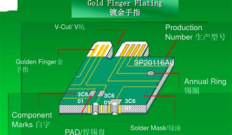
The PCB substrate and solder mask properties directly impact creepage requirements:
- CTI value: As discussed previously
- Surface roughness: Smoother surfaces may require more distance
- Hydrophobicity: Water-repellent properties help
- Flame retardant properties: Important for safety compliance
Standards and Regulations
International Standards Overview
Several key standards govern creepage distance requirements:
- IEC 60950-1 (Information technology equipment)
- IEC 60664-1 (Insulation coordination for low-voltage equipment)
- IPC-2221 (Generic standard on PCB design)
- UL standards (Various product-specific requirements)
Key Standard Requirements
Most standards specify creepage distances based on:
- Voltage levels (typically in ranges)
- Pollution degree
- Material group (CTI-based)
- Altitude considerations
For example, IEC 60664-1 provides detailed tables specifying minimum creepage distances for various combinations of these factors.
Calculating Requirements
A simplified approach to determining creepage distance:
- Determine working voltage (RMS for AC, DC for DC)
- Identify pollution degree
- Determine material CTI group
- Consult appropriate standard tables
- Apply altitude correction if needed (>2000m)
Example calculation:
- 250V RMS, Pollution Degree 2, Material Group IIIa → ~2.5mm creepage (per IEC 60664-1)
Practical Implementation in PCB Design
Layout Techniques for Adequate Creepage
Effective strategies to meet creepage requirements:
- Slotting: Cutting slots in PCB to increase surface path
- Barrier ribs: Creating raised insulation barriers
- Conformal coating: Applying protective coatings to enhance surface insulation
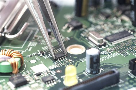
- Proper component placement: Strategic arrangement of high-voltage components
- Solder mask utilization: Ensuring complete coverage in critical areas
Common Pitfalls and Mistakes
Frequent errors in creepage implementation:
- Ignoring solder mask misalignment tolerances
- Not accounting for manufacturing tolerances
- Overlooking creepage paths under components
- Neglecting edge clearance requirements
- Failing to consider assembly variations
Design Verification Methods
Techniques to verify creepage compliance:
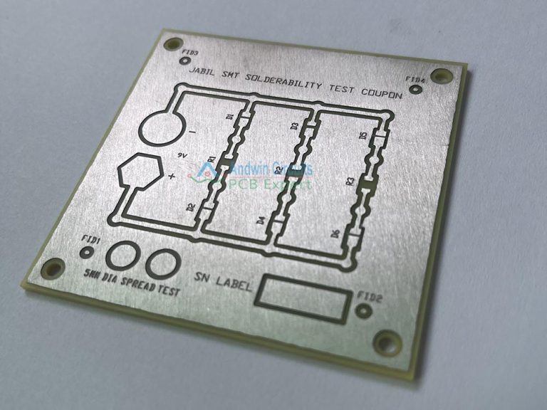
- Visual inspection: Manual measurement of critical paths
- DFM checks: Using design rule checks (DRC) with creepage rules
- 3D modeling: Advanced CAD tools can measure surface paths
- Prototype testing: Hi-pot testing for verification
Advanced Considerations
High Voltage Design Challenges
Special considerations for high voltage PCBs (>1kV):
- Non-linear increase in requirements at higher voltages
- Importance of rounded conductor edges to reduce field concentration
- Need for corona-free designs
- Specialized materials with higher CTI values
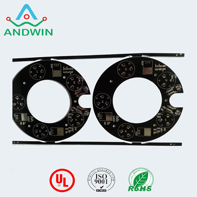
High Density Design Solutions
Balancing creepage requirements with miniaturization:
- Use of higher CTI materials to reduce distances
- Strategic use of conformal coatings
- Innovative insulation barriers
- Multi-layer board optimization
Altitude Compensation
Adjusting for high altitude operation:
- Standard requirements typically for ≤2000m
- Above 2000m, derating factors apply (typically 1.13x per 1000m)
- May require increased distances or enhanced insulation
Future Trends and Developments
Material Innovations
Emerging materials affecting creepage design:
- Nano-composite insulating materials
- Super-hydrophobic coatings
- Self-healing insulation materials
- High CTI engineered thermoplastics
Design Automation
Advancements in CAD tools:
- Automated creepage path calculation
- Real-time DRC for safety spacing
- 3D creepage analysis
- Integration with component libraries
Standard Evolution
Changing regulatory landscape:
- Harmonization of international standards
- Updates for new technologies (EV, renewable energy, etc.)
- Addressing miniaturization challenges
- Climate change considerations (higher humidity, pollution)
Conclusion
Proper understanding and implementation of creepage distance requirements form a cornerstone of safe and reliable PCB design. By considering voltage levels, environmental conditions, material properties, and applicable standards, designers can create products that meet safety requirements while optimizing performance and cost.
As electronic devices continue to evolve with higher power densities and more challenging operating environments, the importance of creepage distance considerations will only increase. Designers must stay informed about material advancements, design techniques, and regulatory updates to ensure their products remain safe and compliant throughout their operational life.
The careful application of creepage distance principles ultimately contributes to the prevention of electrical failures, protection of end-users, and enhancement of product reliability – making it an indispensable aspect of professional PCB design practice.