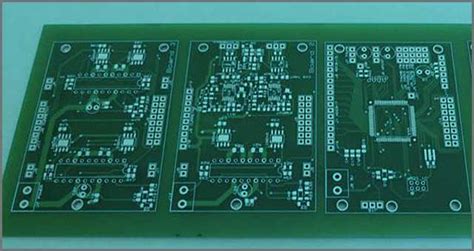
Understanding high frequency pcb design
Key Principles Of High Frequency PCB Design
High frequency PCB design is a specialized area within the broader field of printed circuit board engineering, requiring a deep understanding of both electrical and material properties to ensure optimal performance.
One of the key principles in high frequency PCB design is the management of signal integrity.
At high frequencies, signals can degrade due to various factors such as impedance mismatches, crosstalk, and electromagnetic interference (EMI). To mitigate these issues, designers must carefully consider the layout and routing of traces. For instance, maintaining consistent trace widths and using controlled impedance traces can help preserve signal integrity by minimizing reflections and losses.
Another critical aspect is the selection of materials.
The dielectric constant (Dk) and loss tangent (Df) of the substrate material significantly impact the performance of high frequency circuits. Materials with low Dk and Df values are preferred as they reduce signal attenuation and phase distortion. Additionally, the choice of copper foil type and thickness can influence the skin effect, where high frequency currents tend to flow on the surface of conductors, thereby affecting resistance and inductance. Therefore, selecting appropriate materials is essential for achieving the desired electrical performance.
Thermal management is also a crucial consideration in high frequency PCB design.
High frequency circuits often generate substantial heat, which can affect both the performance and reliability of the PCB. Effective thermal management strategies, such as the use of thermal vias, heat sinks, and proper component placement, are necessary to dissipate heat efficiently. Moreover, understanding the thermal properties of the materials used, including their thermal conductivity and coefficient of thermal expansion, is vital to prevent thermal stress and potential damage to the PCB.
Grounding and power distribution play a significant role in high frequency PCB design as well.
A well-designed ground plane can provide a low impedance path for return currents, reducing noise and improving signal integrity. Additionally, proper decoupling and bypass capacitors are essential to filter out high frequency noise from the power supply, ensuring stable operation of the circuit. The placement of these capacitors close to the power pins of active components can further enhance their effectiveness.
Furthermore, electromagnetic compatibility (EMC) is a major concern in high frequency PCB design.
To minimize EMI, designers must implement shielding techniques and follow best practices for trace routing. For example, differential pairs should be routed together to cancel out common-mode noise, and traces carrying high frequency signals should be kept away from sensitive analog circuits. Additionally, the use of ground fills and stitching vias can help contain electromagnetic fields and reduce radiation.
Simulation and modeling tools are indispensable in high frequency PCB design.
These tools allow designers to predict the behavior of their circuits under various conditions, enabling them to identify and address potential issues before fabrication. By simulating signal integrity, thermal performance, and EMC, designers can optimize their designs for better performance and reliability.
In conclusion, high frequency PCB design is a complex and multifaceted discipline that requires careful consideration of various factors to ensure optimal performance. By understanding and applying key principles such as signal integrity management, material selection, thermal management, grounding and power distribution, and EMC, designers can create high frequency PCBs that meet the stringent demands of modern electronic applications. The use of advanced simulation and modeling tools further enhances the design process, enabling the development of robust and reliable high frequency circuits.
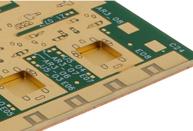
Material Selection For High Frequency PCBs
When designing high frequency printed circuit boards (PCBs), the selection of materials plays a pivotal role in ensuring optimal performance and reliability. High frequency PCBs are typically used in applications such as telecommunications, radar systems, and advanced computing, where signal integrity and minimal loss are paramount. Therefore, understanding the properties and implications of various materials is essential for engineers and designers.
To begin with, the dielectric constant (Dk) of the substrate material is a critical factor.
The dielectric constant affects the speed at which signals propagate through the PCB. Materials with a low Dk are preferred for high frequency applications because they allow signals to travel faster and with less distortion. Common materials with low dielectric constants include PTFE (Polytetrafluoroethylene), also known as Teflon, and certain ceramic-filled laminates. These materials are specifically engineered to provide stable dielectric properties over a wide range of frequencies and temperatures.
In addition to the dielectric constant, the dissipation factor (Df) is another important parameter.
The dissipation factor measures the amount of energy lost as heat in the dielectric material. For high frequency PCBs, a low dissipation factor is desirable to minimize signal loss and maintain signal integrity. Materials such as Rogers RO3000 and RO4000 series laminates are often chosen for their low dissipation factors, which contribute to reduced signal attenuation and improved overall performance.
Thermal management is another crucial consideration in high frequency PCB design.
High frequency signals can generate significant amounts of heat, which can affect the performance and longevity of the PCB. Therefore, materials with good thermal conductivity are essential to dissipate heat effectively. Copper-clad laminates with high thermal conductivity, such as those containing ceramic fillers, are commonly used to enhance heat dissipation. Additionally, the coefficient of thermal expansion (CTE) of the material must be compatible with other components to prevent mechanical stress and potential failure during thermal cycling.
Furthermore, the surface finish of the PCB material can impact signal integrity at high frequencies.
Surface finishes such as Electroless Nickel Immersion Gold (ENIG) and Immersion Silver are often preferred for their excellent conductivity and smooth surface, which help to reduce signal loss and improve performance. These finishes also provide good corrosion resistance, which is important for maintaining long-term reliability in harsh environments.
The choice of material also influences the manufacturability and cost of the PCB.
High performance materials like PTFE and ceramic-filled laminates can be more challenging to process and may require specialized fabrication techniques. This can increase production costs and lead times. Therefore, it is important to balance performance requirements with manufacturability and cost considerations. Collaborating with experienced PCB manufacturers can help in selecting materials that meet both performance and budgetary constraints.
In conclusion, material selection is a fundamental aspect of high frequency PCB design that directly impacts signal integrity, thermal management, and overall performance. By carefully considering factors such as dielectric constant, dissipation factor, thermal conductivity, surface finish, and manufacturability, designers can optimize their high frequency PCBs for demanding applications. As technology continues to advance, ongoing research and development in PCB materials will undoubtedly lead to even more sophisticated solutions, further enhancing the capabilities of high frequency electronic systems.
Signal Integrity Challenges In High Frequency PCB Design
In the realm of high frequency PCB design, signal integrity challenges are paramount and demand meticulous attention. As frequencies escalate, the behavior of signals becomes increasingly complex, necessitating a deep understanding of various factors that can compromise signal integrity.
One of the primary challenges is the phenomenon of signal reflection, which occurs when a signal encounters an impedance discontinuity.
This can lead to signal degradation, as portions of the signal are reflected back towards the source, causing interference and potential data corruption. To mitigate this, designers must ensure impedance matching throughout the PCB, which involves carefully selecting and controlling the materials and geometries of the traces.
Another significant challenge is crosstalk, which arises when signals in adjacent traces interfere with each other.
This is particularly problematic in high frequency designs where the close proximity of traces can lead to unwanted coupling. Crosstalk can manifest as noise, leading to errors in signal interpretation. To address this, designers often employ techniques such as increasing the spacing between traces, using differential signaling, and incorporating ground planes to provide a return path for signals and reduce electromagnetic interference.
Moreover, the issue of signal attenuation cannot be overlooked.
As signals travel through the PCB, they can lose strength due to the resistive and dielectric losses in the materials. This attenuation is more pronounced at higher frequencies, where the skin effect causes current to flow primarily on the surface of conductors, increasing resistance. To combat this, designers may use low-loss materials and optimize trace widths to balance between minimizing resistance and maintaining manageable trace dimensions.
In addition to these challenges, electromagnetic interference (EMI) poses a significant threat to signal integrity in high frequency PCB design.
EMI can originate from both external sources and internal components, leading to disruptions in signal transmission. Shielding and proper grounding are critical strategies to mitigate EMI. By enclosing sensitive components in conductive enclosures and ensuring a robust grounding scheme, designers can significantly reduce the impact of EMI on signal integrity.
Furthermore, the layout of the PCB plays a crucial role in maintaining signal integrity.
The placement of components, routing of traces, and the design of power and ground planes must be carefully considered. For instance, placing high-speed components close to each other and minimizing the length of high-frequency signal paths can reduce the potential for signal degradation. Additionally, the use of via stitching and careful layer stack-up design can enhance the performance of the PCB by providing consistent impedance and reducing the risk of signal reflection and crosstalk.
Thermal management is another aspect that intersects with signal integrity challenges.
High frequency components often generate significant heat, which can affect the performance and reliability of the PCB. Effective thermal management techniques, such as the use of thermal vias, heat sinks, and proper airflow design, are essential to ensure that the PCB operates within safe temperature limits, thereby preserving signal integrity.
In conclusion, high frequency PCB design presents a myriad of signal integrity challenges that require a comprehensive and nuanced approach. By addressing issues such as signal reflection, crosstalk, attenuation, EMI, and thermal management, designers can enhance the performance and reliability of their PCBs. Through careful planning, material selection, and layout optimization, it is possible to mitigate these challenges and achieve robust high frequency designs that meet the stringent demands of modern electronic applications.
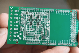
Best Practices For Layout And Routing In High Frequency PCBs
Understanding high frequency PCB design requires a meticulous approach to layout and routing to ensure optimal performance and signal integrity. High frequency circuits, typically operating at frequencies above 1 GHz, are highly sensitive to layout and routing practices. Therefore, adhering to best practices is crucial to mitigate issues such as signal loss, electromagnetic interference (EMI), and crosstalk.
One of the fundamental principles in high frequency PCB design is maintaining controlled impedance.
Controlled impedance ensures that the signal traces have a consistent impedance, which is critical for minimizing signal reflections and maintaining signal integrity. To achieve this, designers must carefully select the trace width, spacing, and the dielectric material of the PCB. Utilizing impedance calculators and simulation tools can aid in determining the appropriate parameters for the specific frequency and signal requirements.
In addition to controlled impedance, minimizing signal path lengths is essential.
Longer signal paths can introduce delays and increase the likelihood of signal degradation. Therefore, it is advisable to keep the signal paths as short and direct as possible. This practice not only reduces the potential for signal loss but also helps in minimizing the loop area, which is beneficial for reducing EMI.
Another key aspect of high frequency PCB design is the use of proper grounding techniques.
A solid ground plane is indispensable for providing a low impedance return path for high frequency signals. This helps in reducing noise and improving signal integrity. It is also important to ensure that the ground plane is continuous and unbroken, as any gaps can lead to increased inductance and potential signal integrity issues. Additionally, placing decoupling capacitors close to the power pins of high frequency components can help in filtering out noise and stabilizing the power supply.
When it comes to routing high frequency signals, differential pairs are often employed.
Differential signaling involves using two complementary signals to transmit data, which can significantly reduce EMI and crosstalk. It is crucial to route differential pairs together, maintaining equal lengths and consistent spacing to ensure that the signals remain synchronized. Any mismatch in length or spacing can lead to signal skew and degrade the performance of the differential pair.
Furthermore, the use of vias should be minimized in high frequency PCB design.
Vias introduce parasitic inductance and capacitance, which can adversely affect signal integrity. If vias are unavoidable, it is important to use them judiciously and ensure that they are properly back-drilled to remove any unused stubs that can act as resonant structures.
Incorporating proper shielding techniques is also beneficial in high frequency PCB design.
Shielding can help in isolating sensitive signals from external noise sources and preventing EMI from affecting other parts of the circuit. This can be achieved through the use of ground planes, metal enclosures, or even dedicated shielding layers within the PCB stack-up.
Lastly, thorough testing and validation are imperative in high frequency PCB design.
Signal integrity analysis, such as time-domain reflectometry (TDR) and vector network analysis (VNA), can provide valuable insights into the performance of the PCB. These tests can help identify any potential issues and allow for necessary adjustments to be made before finalizing the design.
In conclusion, best practices for layout and routing in high frequency PCBs revolve around maintaining controlled impedance, minimizing signal path lengths, employing proper grounding techniques, using differential pairs, minimizing vias, incorporating shielding, and conducting thorough testing. By adhering to these principles, designers can ensure that their high frequency PCBs perform reliably and efficiently, meeting the stringent demands of modern electronic applications.