Understanding Multilayer Printed Circuit Boards and Their Benefits
Key Takeaways
When considering the shift to multilayer printed circuit boards (PCBs), it’s essential to understand their multi-faceted structure and the benefits they provide. Multilayer PCBs are composed of several layers of circuitry, which allows them to house a greater number of components within a compact design. This complexity can pose challenges, but it also enables manufacturers to meet the escalating demands of modern electronics, such as mobile devices and advanced communication systems.
One significant aspect that you will encounter is the importance of selecting the right materials for your PCB manufacturing needs. Various materials contribute to different electrical and thermal properties that can impact performance. Additionally, consolidating multiple functions onto a single multilayer PCB can significantly reduce the overall PCB manufacturing cost, as it simplifies assembly processes and minimizes space requirements in your devices.
Understanding the applications is also key; these PCBs are employed in everything from consumer electronics to automotive systems, providing enhanced reliability and performance. Depending on your specifications or custom requirements, exploring relationships with established PCB manufacturing companies will help you find solutions best suited for your projects. In conclusion, embracing multilayer designs not only fosters innovation but also represents a strategic business decision that can elevate your PCB manufacturing business by enhancing product capabilities while streamlining costs.
| Topic | Key Points |
|---|---|
| Structure | Multiple layers enabling compact designs |
| Complexity | Challenging yet essential for advanced applications |
| Material Selection | Impact on electrical and thermal properties |
| Applications | Wide-ranging use in modern electronics |
| Cost-Effectiveness | Reducing assembly costs by consolidating functions |
Incorporating multilayer PCB technology could be pivotal for staying competitive in today’s rapidly evolving market landscape.

Understanding the Structure of Multilayer Printed Circuit Boards
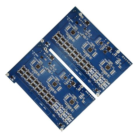
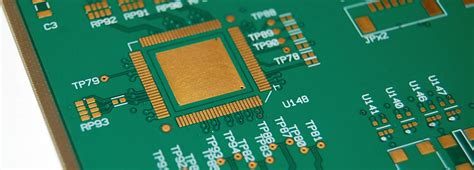
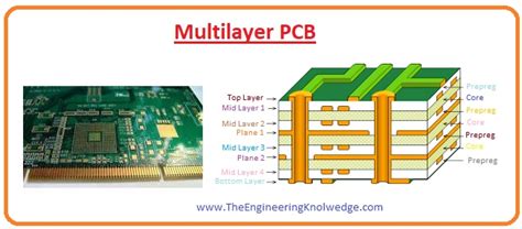
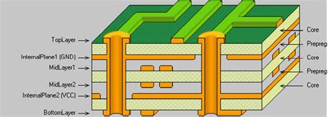
Multilayer printed circuit boards (PCBs) are intricate assemblies designed to meet the growing demands of modern electronics. Their structure typically consists of three or more conductive layers separated by insulating layers, allowing for a compact design that packs a significant amount of circuitry into a small space. You may find that each layer serves a specific function, enabling complex routing and reducing electromagnetic interference. This multilayer arrangement not only increases the density of the electronic components but also enhances electrical performance significantly. When evaluating pcb manufacturing options, you should consider how these layered designs influence performance and reliability.
The pcb manufacturing companies you choose will often emphasize the complexities involved in creating multilayer boards, noting how they require precise alignment and advanced techniques during assembly. These complexities can impact the overall cost; hence understanding pcb manufacturing cost is essential for budgeting your projects effectively. In addition to minimizing space and weight, multilayer designs offer better thermal management, which is increasingly vital for today’s high-performance electronics.
Moreover, if you’re considering venturing into the pcb manufacturing business, grasping the structural aspects of multilayer PCBs will help you identify opportunities and differentiate your offerings in a competitive market. Whether you’re an engineer focused on design or a business professional in manufacturing, an awareness of these structures will ultimately lead to more innovative and effective electronic solutions. For more information on PCB assembly services, visit Andwin PCB.
The Complexity of Multilayer PCB Designs
Multilayer printed circuit boards (PCBs) are essential components in modern electronics, characterized by their intricate construction and the need for precise engineering. As you delve into the world of multilayer PCB designs, you will discover that their complexity arises from the need to layer multiple conductive paths within a limited space. Each additional layer amplifies both the challenge and potential of the design, as you must consider factors such as signal integrity, thermal management, and component placement. When working with PCB manufacturing companies, understanding these complexities is vital, as they directly influence the PCB manufacturing cost. A well-designed multilayer board can accommodate advanced functionalities, paving the way for innovations in various devices—from smartphones to sophisticated industrial equipment. In your dealings or considerations related to a PCB manufacturing business, it is crucial to recognize that proper planning and execution in the multilayer design phase can lead to significant performance benefits, reducing errors and enhancing durability. By grasping these design intricacies, you position yourself better to make informed choices that align with your electronic project’s objectives.
Materials Used in Multilayer PCBs
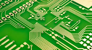
When it comes to multilayer printed circuit boards (PCBs), the selection of materials plays a crucial role in determining the overall performance and reliability of the final product. Generally, you will encounter materials such as FR-4—a composite made from woven fiberglass cloth and epoxy resin—which is the most widely used substrate for PCBs due to its excellent balance of electrical insulation and thermal properties. Additionally, polyimide is an alternative choice that offers superior thermal stability and flexibility, making it ideal for flexible multilayer applications. The metals chosen for trace layers, such as copper, are also vital; they facilitate effective electrical conduction while impacting the total pcb manufacturing cost significantly.
When analyzing materials for multilayer PCBs, you may want to take a closer look at their specific dielectric constants, which influence signal integrity and are particularly critical in high-speed applications. This is where understanding both substrate materials and conductive layers becomes essential when working with various pcb manufacturing companies to ensure they can meet your specifications. Moreover, while evaluating potential suppliers and the overall pcb manufacturing business, consider how they handle material sourcing and whether they offer sustainable options—this can enhance both performance and marketability.
“Always prioritize material selection; it sets the foundation for your PCB’s performance.”
Incorporating diverse materials not only enhances electrical performance but also enables intricate designs that cater to advanced electronic needs. By selecting high-quality components thoughtfully, you ensure that your multilayer boards perform effectively across various applications.
Applications of Multilayer Printed Circuit Boards in Modern Electronics
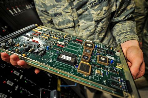
Multilayer printed circuit boards (PCBs) have become integral to modern electronics, catering to a wide array of applications across various industries. These versatile designs allow you to pack more functionality and complexity into a compact space, which is especially valuable in devices such as smartphones, tablets, laptops, and medical equipment. The ability to interconnect multiple layers significantly reduces the overall footprint of your electronic devices while enhancing their performance. Furthermore, pcb manufacturing companies ensure that these advanced designs maintain high levels of reliability and efficiency.
In the automotive industry, multilayer PCBs are critical for the advancement of electric vehicles and autonomous driving technologies. Their capacity to handle complex signal processing and power management systems makes them ideal for applications such as advanced driver-assistance systems (ADAS) and electronic control units (ECUs). Similarly, in the telecommunications sector, multilayer PCBs enable faster data transmission rates essential for 5G networks. The increasing demand for miniaturization in consumer electronics is pushing the pcb manufacturing sector to innovate continually. This has resulted in a competitive landscape where pcb manufacturing cost must align with enhanced capabilities without compromising quality.
Moreover, industries that rely on IoT devices are also leaning towards multilayer PCBs to achieve compactness while supporting numerous components on a single board. As your project evolves toward greater complexity and functionality, recognizing the potential applications of multilayer designs will empower you to meet contemporary electronic needs more effectively. Balancing performance with cost is paramount for any pcb manufacturing business, thereby making multilayer options not just a choice but a necessity for cutting-edge electronic solutions.

Benefits of Using Multilayer PCBs for Electrical Performance
Multilayer printed circuit boards (PCBs) offer numerous benefits that significantly enhance electrical performance in various electronic applications. One of the primary advantages of multilayer PCBs is their ability to reduce the size and weight of electronic devices while maintaining high performance. By stacking multiple layers, you can achieve greater circuit density, leading to more compact designs. This not only saves space but also improves the electrical performance by reducing the length of connections, which helps in minimizing signal loss and interference.
Furthermore, multilayer PCBs facilitate better heat dissipation, a critical factor in modern electronics where devices operate at higher power levels. The use of advanced materials in pcb manufacturing enhances thermal management capabilities, ensuring that components remain within optimal temperature ranges during operation. Consequently, this can lead to increased reliability and longevity of electronic products.
In addition to these performance enhancements, multilayer designs allow for improved routing options for complex circuitry. This flexibility is a significant benefit when dealing with dense layouts found in high-tech devices such as smartphones, tablets, and advanced computing systems. Consequently, you will find that partnering with reputable pcb manufacturing companies often leads to custom solutions that meet precise specifications for your electrical requirements.
Although pcb manufacturing costs can be higher for multilayer boards compared to simpler designs, the investment often pays off in terms of improved functionality and efficiency. The benefits that multilayer PCBs bring to your projects—such as enhanced electrical performance and compact designs—make them a preferred choice for any pcb manufacturing business focused on delivering high-quality electronic solutions. Overall, considering these factors will help you make informed decisions when selecting PCB designs tailored to your unique needs in today’s competitive electronics market.
Innovations in Multilayer PCB Manufacturing Techniques
In the rapidly evolving world of multilayer printed circuit boards (PCBs), innovations in pcb manufacturing techniques play a crucial role in meeting the ever-increasing demands of modern electronics. One notable advancement is the shift towards more efficient pcb manufacturing companies that leverage cutting-edge technologies such as automation and advanced materials. These companies are constantly striving to reduce pcb manufacturing costs while enhancing the quality and reliability of their products. For instance, improved layering techniques allow for thinner yet more robust designs, which are integral to accommodating the compact nature of modern electronic devices. Additionally, innovations like laser direct imaging (LDI) and automated optical inspection (AOI) have significantly increased precision in the manufacturing process, reducing errors and improving yield rates. By staying updated with these advancements, you can ensure that your multilayer PCB designs not only meet performance standards but also fit within your budget constraints, ultimately strengthening your pcb manufacturing business presence in a competitive marketplace. As these techniques continue to evolve, they open up new possibilities for your designs, pushing the boundaries of what is feasible in electronic applications.
Challenges Associated with Designing Multilayer PCBs
Designing multilayer printed circuit boards (PCBs) presents a variety of challenges that can impact both the pcb manufacturing process and the overall performance of the final product. One significant challenge is achieving optimal layer stacking—this requires careful planning to ensure that the layer configuration supports signal integrity and minimizes electromagnetic interference. Additionally, as you incorporate more layers, the pcb manufacturing cost may increase due to the added complexity in both design and production processes. This can be especially pertinent for smaller pcb manufacturing companies that may struggle to balance quality and affordability in their offerings.
Another concern is ensuring adequate thermal management; with multiple layers, heat dissipation can become an issue, necessitating innovative design solutions to prevent overheating in densely packed assemblies. Furthermore, the choice of materials becomes critical as you need to select substrates that not only suffice for electrical properties but also match cost-efficient standards for your pcb manufacturing business. Ultimately, understanding these challenges enables you to make informed decisions that enhance not just the manufacturability but also the longevity and performance of your multilayer PCBs.
Conclusion
In summary, multilayer printed circuit boards (PCBs) play a crucial role in the advancement of modern electronics. Their complex structure allows for the integration of multiple layers, enhancing circuit density and improving electrical performance. By utilizing a variety of materials and innovative pcb manufacturing techniques, you can achieve designs that meet high standards of efficiency and functionality. When considering pcb manufacturing companies, it’s essential to evaluate their experience and capabilities to ensure they can deliver quality products that align with your specific needs. The pcb manufacturing cost can vary, but investing in multilayer designs often results in significant long-term benefits for your pcb manufacturing business by facilitating more complex electronic applications while reducing the size and complexity of overall systems. As technology continues to evolve, understanding the advantages and intricacies of multilayer PCBs becomes ever more important for those who wish to stay ahead in the competitive electronics landscape.
FAQs
What are multilayer printed circuit boards (PCBs) and how do they differ from single-layer boards?
Multilayer PCBs consist of two or more conductive layers separated by insulating material, which allows for more complex circuitry compared to single-layer PCBs. This multi-layered structure significantly enhances electrical performance.
What are the main benefits of using multilayer PCBs in electronic design?
The primary benefits include improved signal integrity, reduced electromagnetic interference, and the ability to fit complex circuit designs into a compact space, all of which are crucial in today’s advanced electronics.
How does the complexity of multilayer PCB designs affect the manufacturing process?
The increased complexity demands precise engineering and sophisticated pcb manufacturing techniques, often leading to higher pcb manufacturing costs due to the need for specialized machinery and skilled labor.
What materials are typically used in multilayer PCBs?
Common materials include fiberglass for insulation, copper for conductive layers, and various laminates suited for specific thermal and electrical properties necessary in high-performance applications.
Where can I find reliable PCB manufacturing companies?
You can research various pcb manufacturing companies, focusing on their experience, client reviews, and certifying standards to ensure quality during your project.
How can I reduce the overall PCB manufacturing cost?
To lower your overall pcb manufacturing cost, consider simplifying your design where possible or partnering with established manufacturers who offer competitive pricing based on volume production.