Understanding OSP (Organic Solderability Preservative) in PCB Manufacturing
Introduction to OSP in PCB Fabrication
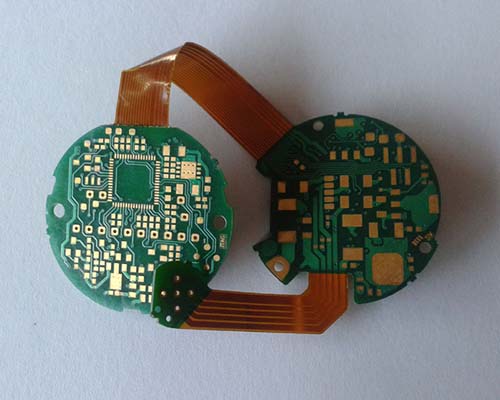
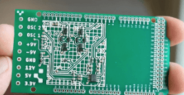
Printed Circuit Boards (PCBs) are the backbone of modern electronics, providing mechanical support and electrical connections for electronic components. One critical aspect of PCB manufacturing is ensuring the solderability of copper pads, which directly impacts the reliability of solder joints during assembly. Among various surface finishes available, Organic Solderability Preservative (OSP) has gained popularity due to its cost-effectiveness, environmental friendliness, and compatibility with fine-pitch components.
This article explores OSP in detail, covering its composition, advantages, disadvantages, application process, and comparison with other PCB surface finishes. By the end, readers will have a comprehensive understanding of OSP’s role in PCB manufacturing.
What is OSP (Organic Solderability Preservative)?
OSP is a water-based, organic coating applied to exposed copper pads on a PCB to prevent oxidation before soldering. It forms a thin, protective layer that maintains solderability while being environmentally safer than some alternatives like HASL (Hot Air Solder Leveling) or ENIG (Electroless Nickel Immersion Gold).
Composition of OSP
OSP coatings typically consist of:
- Benzotriazole (BTA) or related organic compounds.
- Azole-based chemicals that bond with copper.
- Anti-corrosion additives to enhance shelf life.
The coating is ultra-thin (0.2–0.5 μm) and transparent, making it difficult to visually inspect but highly effective in preserving copper surfaces.
Advantages of OSP in PCB Manufacturing
1. Cost-Effective Solution
OSP is one of the most economical surface finishes, making it ideal for high-volume production where cost efficiency is crucial.
2. Flat Surface for Fine-Pitch Components
Unlike HASL, which can create uneven surfaces, OSP provides a flat, uniform coating, essential for fine-pitch and Ball Grid Array (BGA) components.
3. Environmentally Friendly
OSP does not contain heavy metals (e.g., lead or nickel) and is RoHS-compliant, making it a sustainable choice.
4. Excellent Solderability
When properly stored and handled, OSP-coated PCBs offer reliable solderability, forming strong intermetallic bonds during reflow soldering.
5. Simple Application Process
The OSP coating process is straightforward compared to ENIG or immersion silver, requiring fewer chemical steps.
Disadvantages of OSP
Despite its benefits, OSP has some limitations:
1. Limited Shelf Life
OSP-coated PCBs typically have a shelf life of 6–12 months (depending on storage conditions). Beyond this period, oxidation may degrade solderability.
2. Sensitive to Handling
The organic layer can be easily damaged by fingerprints or mechanical abrasion, requiring careful handling during assembly.
3. Not Suitable for Multiple Reflow Cycles
OSP decomposes after the first reflow cycle, making it less ideal for double-sided assembly unless handled carefully.
4. Difficult to Inspect
Since OSP is transparent, visual inspection for defects is challenging, requiring specialized equipment.
OSP Application Process in PCB Manufacturing
The OSP coating process involves several key steps:
Step 1: Cleaning the Copper Surface
- PCBs undergo acid cleaning and micro-etching to remove oxides and contaminants.
Step 2: Pre-Dip Treatment
- A mild acid solution prepares the copper for optimal OSP adhesion.
Step 3: OSP Coating
- The PCB is immersed in an OSP solution, forming a molecular bond with copper.
Step 4: Drying
- The board is dried to solidify the OSP layer.
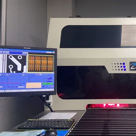
Step 5: Quality Inspection
- Electrical testing and solderability checks ensure coating uniformity.
Comparison of OSP with Other PCB Surface Finishes
| Surface Finish | Advantages | Disadvantages | Best Use Cases |
|---|---|---|---|
| OSP | Low cost, flat surface, eco-friendly | Limited shelf life, sensitive handling | Consumer electronics, cost-sensitive applications |
| HASL (Lead-Free) | Durable, long shelf life | Uneven surface, thermal stress | General-purpose PCBs |
| ENIG (Electroless Ni/Immersion Au) | Excellent solderability, flat surface | Expensive, risk of black pad | High-reliability applications (medical, aerospace) |
| Immersion Silver | Good for fine-pitch, moderate cost | Tarnishes over time | RF and high-speed designs |
| Immersion Tin | Flat surface, good for press-fit pins | Prone to whiskering | Automotive and industrial PCBs |
Best Practices for Using OSP-Coated PCBs
To maximize OSP performance, follow these guidelines:
- Proper Storage
- Store PCBs in nitrogen-sealed bags with desiccants to prevent oxidation.
- Use within 6 months for optimal solderability.
- Careful Handling
- Avoid touching copper pads directly to prevent contamination.
- Use gloves and ESD-safe packaging.
- Optimized Soldering Profile
- Ensure proper reflow temperature (peak ~240–250°C) to fully activate OSP.
- Avoid Multiple Reflows
- If double-sided assembly is needed, complete it in a single reflow cycle if possible.
Future Trends in OSP Technology
As PCB technology evolves, OSP is also improving:
- Enhanced formulations with longer shelf life.
- Hybrid coatings combining OSP with nano-materials for better durability.
- Automated inspection systems using AI to detect OSP defects.
Conclusion
OSP is a cost-effective, environmentally friendly, and high-performance surface finish for PCBs, particularly suited for consumer electronics and high-volume production. While it has limitations in shelf life and handling sensitivity, proper storage and process control can mitigate these issues. As technology advances, OSP continues to be a competitive choice against more expensive alternatives like ENIG or immersion silver.
For PCB designers and manufacturers, understanding OSP’s strengths and weaknesses ensures optimal selection for their specific applications, balancing cost, reliability, and performance.