Understanding PCB and PCB Assembly for Modern Electronics
Key Takeaways
Understanding PCB and PCB assembly is fundamental for anyone engaged in modern electronics. These components serve as the backbone of electronic devices, facilitating connections between various electronic elements. The term PCBA, or Printed Circuit Board Assembly, encapsulates the entire process of integrating electronic components onto a PCB, ensuring that each connection is both reliable and efficient. One of the most critical aspects to consider is the design; an optimized PCB layout can significantly enhance device performance, reduce electromagnetic interference, and improve thermal management.
Moreover, attention to detail during the manufacturing and assembly processes can lead to greater reliability in functioning devices. As technology continues to advance, trends such as miniaturization and increased complexity in designs will push manufacturers to innovate in their pcb assembly processes continually.
“In electronics, investing time in robust PCB design and assembly processes often pays dividends in device longevity and performance,” notes an industry expert.
By focusing on these key elements—design considerations, manufacturing efficacy, and assembly techniques—engineers can better appreciate how these factors influence overall product success. Thus, it’s clear that mastering PCB technology is critical not only for building functional devices but also for creating cutting-edge solutions that meet modern-day demands.
Introduction to PCB Technology
Printed Circuit Boards (PCBs) are the backbone of modern electronics, serving as the foundation for connecting various electronic components in devices ranging from smartphones to complex industrial machinery. At their core, PCBs consist of a flat board made from an insulating material, typically fiberglass, with conductive pathways etched onto the surface. These pathways allow electrical signals to travel between different components, facilitating communication and functionality. The significance of PCB assembly (PCBA) cannot be overstated, as it involves the mounting of electronic components onto the PCB, effectively transforming a static board into a fully functional electronic device.
Understanding the nuances of both PCB design and assembly is critical for engineers and manufacturers striving for optimal device performance and reliability. Various factors come into play during this process—such as component placement, soldering techniques, and testing methods—each influencing the overall efficacy of the final product.
Moreover, innovations in materials and assembly technologies continually shape the landscape of PCB manufacturing, enabling smaller, more efficient devices with enhanced functionalities. For example, advancements in surface mount technology (SMT) have significantly improved how components are placed on PCBs, allowing for higher circuit density and reduced manufacturing costs.
Here’s a brief overview of how these concepts interlink:
| Aspect | Description |
|---|---|
| PCBs | Essential substrates for electrical connectivity |
| PCBA | The assembly process that integrates components onto PCBs |
| Component Density | Impacted by technological advancements |
| Manufacturing Cost | Can be reduced through efficient design and assembly methods |
Understanding these connections is crucial not only for developing effective electronic devices but also for ensuring they meet rigorous industry standards. As technology continues to evolve, so too will the strategies employed in PCB design and assembly, further highlighting their indispensable role in driving innovation across multiple sectors.
The Importance of PCB in Modern Electronics
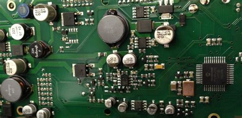
Printed Circuit Boards (PCBs) serve as the backbone of modern electronic devices, providing the essential framework for electrical connections between various components. The intricacies of pcb assembly are vital in ensuring that devices operate efficiently and reliably. In an era characterized by rapid advancements in technology, the design and functionality of PCBs have evolved significantly, catering to the compact size and high performance needed in contemporary electronics. Each layer within a PCB is meticulously designed to accommodate intricate pathways for electricity, which facilitate effective communication between components like microprocessors, sensors, and power supplies. The efficiency of pcba not only affects a device’s functionality but also impacts its thermal management and overall durability. As consumer demand continues to rise for sophisticated technology—ranging from smartphones to home automation systems—manufacturers are increasingly focusing on optimizing PCB designs to improve production processes and enhance device performance. Variations like flexible PCBs have emerged, allowing for innovative arrangements that traditional rigid designs cannot accommodate. Understanding the critical role of pcb assembly is thus imperative for engineers and manufacturers aiming to push the boundaries of what’s possible in modern electronic applications.
Understanding the PCB Manufacturing Process
The PCB manufacturing process is a critical aspect of electronics production that involves several intricate steps, each contributing to the effectiveness and reliability of the final product. Initially, the design phase utilizes specialized software to create a schematic and layout, which serves as the blueprint for constructing the printed circuit board. Once finalized, the design is transferred onto a physical medium through techniques such as photoengraving or laser etching. Following this, conductive traces are added, typically made of copper, which form the electrical pathways that connect various electronic components on the board.
In terms of material selection, different substrates such as FR-4 (a fiberglass epoxy resin) or polyimide are chosen based on their thermal and electrical properties to ensure optimal performance under varying conditions. Subsequently, drilling holes for component insertion is performed with high precision, which is essential for ensuring proper installation during pcb assembly.
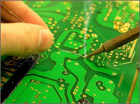
Once these initial steps are completed, processes like surface finish application take place to enhance connectivity and prevent oxidation. This is where pcba, or PCB assembly, comes into play. At this stage, components are affixed to the board using methods such as soldering, which can be achieved either manually or through automated machines like wave soldering and reflow ovens. The goal during this phase is to create reliable joints that can withstand operational stresses.
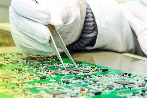
Finally, after assembly is completed, thorough testing procedures are executed to verify both functionality and reliability of the assembled boards. These may include visual inspections as well as electrical tests aimed at identifying any potential defects before the PCBs are integrated into larger electronic systems. The intricacies of each step highlight why understanding every aspect of the PCB manufacturing process, including both design and assembly considerations, is essential for producing electronics that meet rigorous performance standards in today’s technology-driven world.
Key Design Considerations for Effective PCB Assembly
When it comes to pcb assembly, several critical design considerations can significantly impact the overall performance and reliability of the final electronic product. First and foremost, understanding the design specifications is essential. This includes determining the required dimensions, materials, and tolerances for the printed circuit board (PCB) to ensure that it not only meets functional requirements but is also compatible with other components in the assembly process.
Another vital aspect is the layout optimization of circuits within the PCB. A well-optimized layout minimizes electromagnetic interference (EMI) and signal degradation, enhancing overall device performance. Designers must also think about components’ placement; strategically locating high-frequency components can improve signal integrity while optimizing space and performance on the board, crucial for compact electronic devices.
Furthermore, one should consider thermal management within pcb assembly. As devices become smaller and more powerful, heat dissipation becomes a critical concern. Incorporating thermal vias or using heat sinks in strategic areas can help manage temperatures effectively during operation, thus increasing reliability.
Connectivity and soldering methods also play pivotal roles in effective pcba (printed circuit board assembly). Selecting appropriate solder types based on component specifications—such as lead-free options—can further enhance device longevity while ensuring compliance with industry standards.
Ultimately, meticulous attention to these design considerations not only facilitates smoother production but also ensures that the resulting electronics perform efficiently over time. Understanding these factors enables manufacturers to deliver high-quality products that meet consumer expectations in an ever-evolving technological landscape.
The Role of PCB Assembly in Device Performance
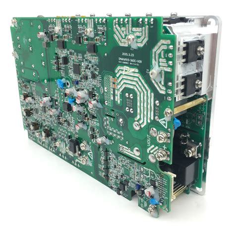
The pcb assembly process plays a pivotal role in determining the overall performance and reliability of electronic devices. At its core, pcba involves the integration of various electronic components onto a printed circuit board, which serves as the backbone for electrical connections and functionality. A well-executed pcb assembly ensures that components such as resistors, capacitors, and integrated circuits are placed accurately and securely, fostering optimal signal integrity and power distribution. In turn, this precision significantly affects the device’s operational efficiency.
Moreover, the design considerations during pcb assembly, such as trace widths and spacing, influence not only electrical performance but also the device’s ability to manage heat dissipation effectively. An intelligently designed pcba can reduce electromagnetic interference (EMI), enhancing the performance of sensitive electronics while maintaining compliance with industry standards. Additionally, manufacturers are increasingly adopting advanced automation technologies to improve accuracy and speed in the pcb assembly process. This evolution is crucial as devices become smaller and more complex, necessitating innovative strategies to maintain performance without compromising reliability.
Ultimately, the quality of pcb assembly directly correlates with device durability; a robust pcba can withstand environmental stresses better than substandard alternatives. Thus, investing in high-quality pcb assembly techniques not only enhances immediate device performance but also supports long-term sustainability in modern electronics—a vital component for success in this ever-evolving market landscape.
Quality Assurance in PCB Production
In the realm of PCB production, quality assurance stands as a pivotal process that significantly influences both the reliability and performance of electronic devices. The implementation of stringent quality control measures throughout the pcb assembly process ensures that each component, from the circuit board layout to the final assembly, meets high standards. Various testing methodologies, such as visual inspections, automated optical inspections (AOI), and electrical testing, play crucial roles in identifying defects early in the production line. By adopting advanced techniques in pcba processes, manufacturers can mitigate risks associated with poor-quality components that might lead to malfunctioning devices or failures during operation. Moreover, consistent adherence to industry standards and certifications reinforces trust among manufacturers and consumers alike, enhancing the overall reputation of electronic products in a competitive market. In summary, a robust quality assurance framework not only safeguards the integrity of PCB production but also contributes substantially to long-term device performance and customer satisfaction.
Innovations in PCB Design and Assembly Techniques
As technology continues to evolve, the field of PCB (Printed Circuit Board) design and pcb assembly is witnessing rapid innovations aimed at enhancing performance, efficiency, and scalability. One key advancement is the adoption of high-density interconnect (HDI) technology, which allows for significantly smaller devices without sacrificing functionality. This technique utilizes finer lines and spaces in the layout, enabling more complex circuit designs packed into smaller footprints. Moreover, the integration of automated assembly processes has transformed traditional pcba practices. Advanced robotics and machines are now able to assemble components with increased precision and speed, reducing the likelihood of human error while improving production rates.
In addition to these advancements, the incorporation of smart manufacturing principles is shaping how PCB assemblies are produced. This includes using data analytics to monitor production processes in real-time for quality assurance and efficiency optimization. As a result, manufacturers can swiftly identify potential issues and implement corrective measures proactively. Furthermore, environmentally friendly materials are gaining traction in both PCB design and assembly processes. Utilizing lead-free solder and sustainable substrates not only meets regulatory requirements but also enhances device reliability.
These innovations are imperative not only for improving manufacturing capabilities but also for responding to market demand for smaller, more efficient electronic devices that maintain high performance standards. The focus on continuous improvement in pcb assembly methods will undoubtedly contribute significantly to the future landscape of electronics manufacturing, ensuring that products are not only cutting-edge but also reliable and sustainable.
Future Trends in PCB and Electronics Manufacturing
As the electronics industry continues to evolve, pcb assembly processes are becoming increasingly sophisticated to meet the demanding needs of contemporary technology. One notable trend is the push towards miniaturization, where PCBs are designed to occupy less space without compromising functionality. This is particularly important in sectors such as mobile communication and wearable technology, where compact designs are essential for user convenience. Additionally, the integration of advanced materials is paving the way for improved performance and reliability; pcba can now utilize flexible substrates that enhance durability while maintaining functionality in various applications.
Another significant trend is the adoption of automation in PCB assembly, which not only increases production efficiency but also reduces human error during manufacturing. Automated systems enable rapid adjustments to the assembly process, allowing manufacturers to adapt quickly to changing market demands or production volumes. Furthermore, as electronics become more interconnected through the Internet of Things (IoT), there is a growing need for PCBs that can support enhanced connectivity and integrated circuits.
Sustainability has also become a key consideration; manufacturers are exploring eco-friendly materials and recycling methods that reduce waste in the production of pcb assembly. This shift towards sustainable practices resonates with consumer demand for greener products and can foster brand loyalty among environmentally conscious customers. All these trends underscore the importance of innovation in both PCB design and assembly, ensuring that modern electronics continue to advance while meeting performance expectations and adhering to environmental standards.
Conclusion
In summary, the interplay between PCB technology and pcb assembly is a cornerstone of modern electronics, serving as the backbone for countless devices we use daily. Understanding the intricacies of the PCBA process—ranging from design considerations to manufacturing techniques—highlights how critical these elements are in ensuring device performance, reliability, and efficiency. As we navigate an increasingly complex technological landscape, innovations in both PCB design and assembly techniques will continue to drive advancements in electronics manufacturing. Ultimately, with stringent quality assurance processes and a keen focus on emerging trends, the future of pcb assembly looks promising. This evolution not only enhances device capabilities but also fosters greater sustainability within the industry. Therefore, stakeholders must remain knowledgeable about these developments to maximize the potential of their electronic products in a competitive market.

FAQs
What is PCB?
A PCB, or Printed Circuit Board, is a foundational component in modern electronics that supports and connects electronic components.
What is PCB assembly?
PCB assembly, often referred to as PCBA, is the process of soldering electronic components onto a PCB to create a functional electronic device.
Why is PCB assembly important?
The quality of pcb assembly directly influences the performance and reliability of electronic devices. A well-executed assembly process ensures that connections are stable, reducing the chances of failure.
What are common methods used in PCB assembly?
Common methods include surface mount technology (SMT) and through-hole technology, each with distinct advantages based on design requirements and component types.
How does design affect PCB assembly?
Proper design considerations, such as component placement and trace routing, can significantly impact the efficiency of the pcb assembly process. A well-designed layout facilitates easier manufacturing and enhances device performance.
What are some challenges faced during PCB assembly?
Challenges include issues like component misalignment, soldering defects, and thermal management during production. Effective quality assurance protocols can help mitigate these risks.
For detailed information about pcb assembly, including advancements in techniques and materials, please visit this link.