Understanding PCB Assembly Processes and Best Practices
Key Takeaways
In the realm of PCB assembly, understanding the nuances of the process is vital for achieving high-quality results. This article emphasizes that successful PCBA relies heavily on attention to detail and adherence to established standards. One major takeaway is the importance of effective communication among team members, which can significantly enhance workflow efficiency. Furthermore, mastering best practices in soldering techniques plays a crucial role in minimizing defects, leading to optimal performance of the assembled boards.
Utilizing essential tools and equipment diligently can also streamline PCB assembly projects. As you progress through the different stages—such as component placement, soldering, and inspection—being well-versed with the tools at your disposal can save time and resources. Quality control measures should not be overlooked; implementing consistent inspection protocols ensures that each assembly meets rigorous standards.
Moreover, acknowledging common challenges in PCBA, such as misalignment and solder bridging, allows teams to devise strategies for overcoming these obstacles. As technology evolves, staying abreast of innovations in PCB assembly will aid in embracing new methodologies that further enhance productivity.
“Continuous improvement in your processes can lead to unprecedented quality and efficiency.”
As you engage with this information, remember that adopting a reflective approach to each PCB assembly project will empower teams to enhance both their skills and outcomes continuously.
Introduction to PCB Assembly: Key Concepts and Terminology
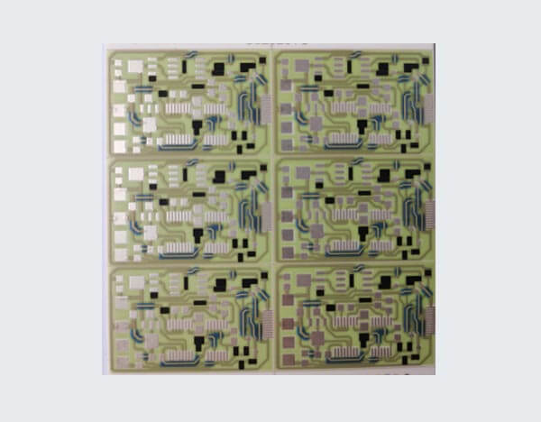
PCB assembly, or PCBA, is a crucial process in the electronics manufacturing industry. It involves the integration of electronic components onto a printed circuit board (PCB) to create a fully functional device. Understanding the key concepts and terminology associated with PCB assembly is essential for anyone involved in electronics design and production. The process starts with the design of the PCB, followed by selecting appropriate components, which are then mounted on the board through various techniques. Common terms related to PCBA include soldering, which refers to the method of joining components to the board using a molten metal alloy, and through-hole and surface-mount technology, which describe different methods of component attachment. Additionally, terms such as bill of materials (BOM), which lists all components required for assembly, and assembly drawings, which provide visual guidance for placement, are fundamental in ensuring an efficient assembly process. By familiarizing oneself with these concepts and terminology, individuals can significantly enhance their PCB assembly projects and ensure that they meet industry standards for quality and performance.
The PCB Assembly Process: Step-by-Step Breakdown
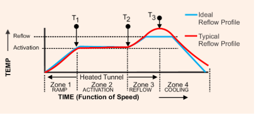
Understanding the pcb assembly process is crucial for achieving high-quality results in your electronic projects. The journey begins with design; a well-crafted schematic lays the foundation for successful pcba (printed circuit board assembly). Following this, the next step involves selecting the appropriate materials, including components, substrates, and solder types. After materials are confirmed, the assembly can commence. Components are placed onto the board, either manually or using automated machines—each method has its advantages. Once positioned, soldering processes are employed; this can be through wave soldering or reflow soldering techniques, depending on whether you are working with surface mount devices or through-hole components. After soldering, it’s imperative to perform thorough inspections to ensure that all connections are secure and that the board meets quality standards. Techniques such as visual inspection and automated optical inspection (AOI) play an essential role in this quality control phase. Finally, functional testing assesses if the assembled pcb performs as intended under simulated working conditions. Overall, understanding these steps ensures that your projects not only meet but exceed performance expectations in today’s fast-paced technology landscape. Each stage in the process is vital for ensuring optimal quality in any pcb assembly project.
Essential Tools and Equipment for Efficient PCB Assembly
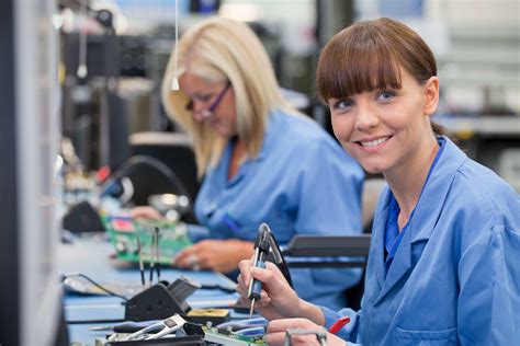
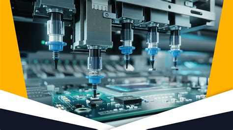
Efficient PCB assembly largely depends on the right selection of tools and equipment tailored for the specific requirements of each project. At the forefront, soldering tools play a vital role, as high-quality soldering can significantly impact the overall performance and reliability of a printed circuit board assembly (PCBA). A reliable soldering iron with adjustable temperature settings is essential to cater to varying solder types and component sensitivities. Moreover, solder paste printers and pick-and-place machines are indispensable for achieving precise alignment and placement of components on the PCB, ultimately enhancing operational efficiency.
In addition to tools aimed at assembly, a solid set of testing equipment is crucial in validating functionality during and after the assembly process. Devices such as multimeters, oscilloscopes, and Automated Optical Inspection (AOI) systems help ensure that each PCBA meets quality standards before deployment. Furthermore, proper handling tools like tweezers and vacuum pickups can prevent damage or misalignment during assembly.
Another important aspect is workspace organization. Having an organized workspace with appropriate storage solutions for components not only improves efficiency but also reduces errors related to misplaced items. It’s essential that all tools are easily accessible for a smooth workflow.
By investing in these essential tools and ensuring that proper techniques are employed throughout the PCB assembly process, teams can produce high-quality PCBAs that meet stringent performance standards while mitigating common assembly-related challenges. This foundation ultimately contributes to efficient project turnaround times and superior product reliability in an ever-evolving electronic landscape.
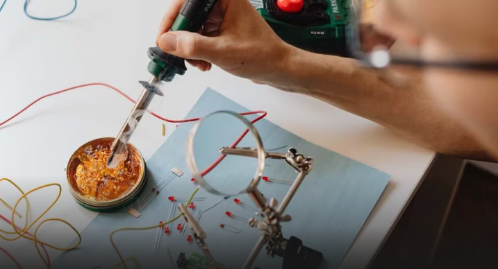
Best Practices for Soldering Techniques in PCB Assembly
In pcb assembly, soldering is a critical process that directly impacts the integrity and functionality of the final product. To achieve optimal results in soldering techniques, it is essential to adhere to a set of best practices that not only improve efficiency but also enhance the overall quality of the printed circuit board assembly (commonly referred to as PCBA). First and foremost, ensuring that all components and pads are clean before soldering is crucial. Contaminants can lead to poor connections and increased failure rates. Additionally, selecting the appropriate solder type, whether leaded or lead-free, can significantly influence the performance of the pcba.
Temperature control during the soldering process is another key factor; maintaining an ideal temperature prevents damage to sensitive components while ensuring a proper bond. It is advisable to use a properly calibrated soldering iron with an appropriate tip size for various joint types to facilitate effective heat transfer. Employing techniques such as proper flux application and minimizing hand movement during soldering helps create stronger joints while avoiding cold joints often associated with insufficient heating.
Moreover, implementing a systematic approach when positioning components can expedite the pcb assembly process. Starting from low-profile parts and progressing toward larger components allows for easier handling and access during assembly. Finally, regular training for personnel on advanced soldering techniques can help maintain high standards across projects, ensuring that each pcba meets or exceeds industry specifications. Ultimately, following these best practices not only enhances the quality of individual assemblies but also contributes positively to overall production efficiency and reliability in PCB assembly projects.
Quality Control Measures in PCB Assembly Projects
Ensuring that pcb assembly processes meet high standards of excellence is critical in the manufacturing of electronic devices. Implementing robust quality control measures during pcba can significantly reduce errors, enhance reliability, and improve overall product performance. One fundamental approach is to establish detailed inspection protocols at various stages of the pcb assembly process. This can include visual inspections to detect soldering defects, misalignments, or component placements that deviate from specifications.
Additionally, utilizing automated optical inspection (AOI) systems can provide real-time feedback, enabling quicker identification of issues and reducing the likelihood of malfunctioning products reaching the market. Another key practice is the adoption of statistical process control (SPC), which uses data collected from the assembly line to monitor and regulate processes, ensuring consistent quality throughout production.
Training personnel on proper soldering techniques and emphasizing the importance of cleanliness and environmental controls within the assembly area can also greatly enhance the quality of the final product. In essence, a holistic approach involving thorough inspections, advanced technologies, and well-trained staff will inherently elevate the standards in pcb assembly projects, addressing common challenges while promoting an ethos of continuous improvement within organizations.
Common Challenges in PCB Assembly and How to Overcome Them
In the realm of PCB assembly (PCBA), several challenges can arise, potentially affecting the overall quality and functionality of the final product. One common issue is the misalignment of components during the assembly process, which can lead to poor solder joints and electrical failures. To mitigate this risk, implementing effective alignment techniques and using automated placement equipment can enhance precision. Another significant challenge is thermal management, as overheating during soldering can damage sensitive components. To address this, maintaining optimal soldering temperatures and employing appropriate cooling methods are essential.
Additionally, contamination of the printed circuit boards can lead to compromised connections and circuit failures. Ensuring a clean workspace and using proper handling techniques will help reduce this risk significantly. Furthermore, a lack of proper documentation regarding assembly processes can create confusion among team members and lead to human error. Standardizing process documentation and providing adequate training can foster consistency and improve assembly outcomes.
Lastly, supply chain disruptions can often pose challenges in acquiring necessary components for PCB assembly (PCBA). Building strong relationships with suppliers and maintaining inventory can help mitigate these risks. By proactively addressing these common challenges with effective strategies, teams engaged in PCB assembly can enhance their workflow efficiency, product quality, and ultimately achieve optimal performance in their projects.
Innovations in PCB Assembly: Emerging Technologies and Trends
The field of pcb assembly is experiencing significant transformations as new technologies emerge, offering innovative solutions to enhance efficiency and quality. One notable trend is the incorporation of automation in the pcb assembly process, which not only accelerates production but also reduces human error, thereby improving overall product quality. Advances in robotics, such as the use of collaborative robots or cobots, are being integrated into assembly lines, enabling more flexible production environments that can quickly adapt to varying workload demands.
Additionally, the integration of machine learning and artificial intelligence into manufacturing systems allows for real-time performance monitoring and predictive maintenance, thus optimizing production timelines. These technologies facilitate quicker identification of potential issues within the pcba workflow, ultimately leading to higher reliability in end products.
Furthermore, advancements in materials science contribute to the development of superior solder compounds that assure stronger joints and better heat dissipation, minimizing failures in electronic devices. The use of innovative printing techniques for solder paste application also marks a leap towards achieving finer pitch components on printed circuit boards without compromising quality.
As these emerging technologies continue to shape the landscape of pcb assembly, staying informed on these trends becomes essential for manufacturers aiming to maintain a competitive edge. By adopting these advancements, industries can expect not only improved efficiency but also enhanced product performance—essential for meeting the growing demands for reliable electronic devices across various sectors.
Conclusion: Future Directions in PCB Assembly Practices
As the world of PCB assembly (pcba) continues to evolve, several trends and innovations are shaping its future. The integration of automation and artificial intelligence into the pcb assembly process enhances precision and efficiency, reducing human error and accelerating production timelines. Additionally, the increasing demand for miniaturization drives manufacturers to explore advanced materials and designs that enable the creation of more compact yet powerful electronics. Sustainability also plays a pivotal role, with companies seeking eco-friendly materials and processes to minimize their environmental impact. The adoption of lean manufacturing principles is another significant trend, focusing on waste reduction and optimized workflows in pcba projects. Furthermore, advancements in inspection technologies are enhancing quality control measures, ensuring that each pcb assembly meets stringent reliability standards. As these innovations unfold, staying informed about best practices and emerging technologies will be crucial for professionals in the industry to maintain a competitive edge in their pcb assembly endeavors.
Conclusion: Future Directions in PCB Assembly Practices
As we look towards the future of PCB assembly (PCBA), it is essential to acknowledge the ongoing developments in the industry that promise to enhance efficiency and reliability. Innovations such as automation and artificial intelligence play a pivotal role in optimizing the PCB assembly process, leading to significant reductions in production times and costs. Moreover, advancements in materials science contribute to higher quality components, facilitating remarkable improvements in performance and long-term durability of electronic devices. Embracing sustainable practices is becoming increasingly vital; thus, many companies are exploring eco-friendly materials and processes within PCBA to minimize environmental impact. The integration of real-time monitoring technologies also offers exciting opportunities for ensuring quality control throughout the assembly process. By adopting these state-of-the-art techniques and best practices, manufacturers can not only meet but exceed market demands while ensuring high standards of quality and efficiency in their PCB assembly projects. As we move forward, staying informed about these trends will be crucial for success in an ever-evolving landscape of electronic manufacturing.
FAQs
What is PCB assembly?
PCB assembly refers to the process of soldering electronic components onto a printed circuit board (PCB) to create a functional electronic circuit. The assembly can range from simple single-layer boards to complex multi-layer designs, often involving various techniques for component placement and soldering.
What are the common techniques used in PCB assembly?
The most common techniques include surface mount technology (SMT) and through-hole technology (THT). SMT involves placing components directly onto the surface of the PCB, while THT requires components to be inserted into pre-drilled holes and soldered from the opposite side.
What equipment is needed for effective PCB assembly?
Essential tools for PCBA include soldering irons, pick-and-place machines, inspection microscopes, and reflow ovens. Each tool plays a specific role in enhancing both efficiency and quality during the pcb assembly process.
How do I ensure quality in my PCB assembly projects?
Implementing rigorous quality control measures, such as visual inspections, automated optical inspection (AOI), and functional testing, is crucial in identifying defects early in the pcb assy process. These practices help in ensuring that end products meet desired specifications.
What challenges might I face during PCB assembly?
Common challenges include misalignment of components, inadequate solder joints, and issues with adhesive materials. Understanding these potential pitfalls allows manufacturers to apply corrective actions effectively and maintain high standards during the pcba process.
For more information on improving your knowledge about PCB assemblies, please click here: Andwin PCB Assembly