Understanding PCB Gerber Files: The Backbone of Modern Electronics Manufacturing
Introduction
In the realm of electronics manufacturing, Printed Circuit Boards (PCBs) are the fundamental building blocks that enable the functionality of virtually all electronic devices. From smartphones and computers to industrial machinery and medical equipment, PCBs are ubiquitous. The design and production of these intricate boards rely heavily on a standardized file format known as the Gerber file. This article delves into the intricacies of PCB Gerber files, exploring their significance, structure, generation, and role in the PCB manufacturing process.
1. The Significance of Gerber Files in PCB Manufacturing
Gerber files serve as the universal language for PCB fabrication. They encapsulate the design data necessary for manufacturers to produce the physical board. Without Gerber files, the transition from a digital design to a tangible PCB would be fraught with errors and miscommunication.
1.1. Historical Context
The Gerber format was developed by Gerber Systems Corp., now a part of Ucamco, in the 1960s. Initially designed for controlling photoplotters, it has evolved to become the de facto standard for PCB data transfer. The format’s longevity and widespread adoption underscore its reliability and adaptability to the evolving needs of the electronics industry.
1.2. Universal Acceptance
One of the primary reasons for the Gerber format’s dominance is its universal acceptance across the PCB manufacturing industry. Regardless of the design software used, Gerber files provide a common ground for designers and manufacturers, ensuring seamless communication and reducing the risk of errors.
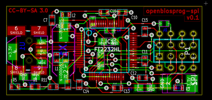
2. The Structure of Gerber Files
Understanding the structure of Gerber files is crucial for both PCB designers and manufacturers. These files are essentially a collection of 2D binary vector images that represent different layers of the PCB.
2.1. File Extensions and Layers
Gerber files typically have extensions like .GBR, .GBX, or .GTL (for top layer), .GBL (for bottom layer), .GTS (for top solder mask), and so on. Each file corresponds to a specific layer of the PCB, such as:
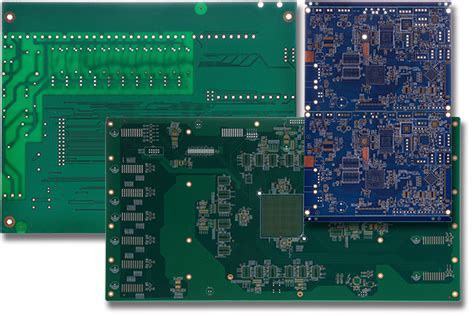
- Copper Layers: These represent the conductive pathways on the PCB. There are usually multiple copper layers, especially in complex multi-layer boards.
- Solder Mask Layers: These define the areas where solder will be applied, protecting the copper traces from oxidation and preventing solder bridges.
- Silkscreen Layers: These contain the component labels, logos, and other markings that aid in assembly and identification.
- Drill Files: While not strictly Gerber files, drill files (often in Excellon format) accompany Gerber files to specify the locations and sizes of holes for through-hole components and vias.
2.2. File Format and Syntax
Gerber files are ASCII-based, making them human-readable to some extent. They consist of a series of commands that define shapes, apertures, and other graphical elements. The syntax includes:
- Aperture Definitions: These specify the shapes and sizes of the drawing tools (apertures) used to create the PCB features.
- Draw and Flash Commands: These commands instruct the photoplotter to draw lines, arcs, or flash (print) predefined shapes at specific locations.
- Coordinate Data: The files contain coordinate data that define the positions of the drawn elements relative to a reference point.
3. Generating Gerber Files
The generation of Gerber files is a critical step in the PCB design process. It involves translating the design data from the PCB design software into the Gerber format.
3.1. Design Software
Most PCB design software, such as Altium Designer, Eagle, KiCad, and OrCAD, includes built-in tools for generating Gerber files. The process typically involves:
- Layer Selection: The designer selects which layers to export, such as copper layers, solder mask, silkscreen, etc.
- Aperture Settings: The software automatically generates aperture definitions based on the design, but designers can customize these settings if necessary.
- File Export: The software exports the selected layers as individual Gerber files, along with a drill file if applicable.
3.2. Verification and Validation
Before sending Gerber files to a manufacturer, it is essential to verify their accuracy. This can be done using Gerber viewers, which allow designers to inspect the files and ensure that all layers align correctly and that there are no missing or erroneous features. Some advanced viewers also offer Design Rule Checking (DRC) to identify potential issues that could affect manufacturability.
4. The Role of Gerber Files in PCB Manufacturing
Gerber files play a pivotal role in the PCB manufacturing process, serving as the blueprint for fabricating the board.
4.1. Photoplotting
The primary use of Gerber files is in photoplotting, a process where the PCB design is transferred onto a photosensitive film. The photoplotter interprets the Gerber files to create precise images of each layer, which are then used to produce the PCB.
4.2. Layer Alignment
In multi-layer PCBs, the alignment of different layers is crucial. Gerber files provide the necessary data to ensure that all layers are perfectly aligned during the lamination process. Misalignment can lead to short circuits, open circuits, or other defects that render the PCB unusable.
4.3. Etching and Plating
The Gerber files guide the etching process, where unwanted copper is removed from the board, leaving only the desired conductive traces. They also inform the plating process, where additional copper is deposited to strengthen the traces and vias.
4.4. Solder Mask and Silkscreen Application
The solder mask and silkscreen layers defined in the Gerber files are used to apply the protective solder mask and the component labels, respectively. These layers enhance the PCB’s durability and usability.
5. Challenges and Considerations
While Gerber files are indispensable in PCB manufacturing, they are not without challenges.
5.1. File Compatibility
Despite the universal acceptance of the Gerber format, there can be compatibility issues between different software and manufacturers. Variations in how software interprets and generates Gerber files can lead to discrepancies. To mitigate this, the industry has adopted the Gerber X2 format, which includes additional metadata to improve clarity and reduce errors.
5.2. Human Error
The generation of Gerber files is a manual process that can be prone to human error. Incorrect layer selection, improper aperture settings, or overlooked design rules can result in faulty PCBs. Rigorous verification and validation processes are essential to minimize these risks.
5.3. File Size and Complexity
As PCBs become more complex, the size and complexity of Gerber files increase. Large files can be challenging to handle, both for designers and manufacturers. Efficient file management and compression techniques are necessary to streamline the process.
6. Future Trends and Developments
The PCB industry is continuously evolving, and so is the Gerber format. Several trends and developments are shaping the future of Gerber files and PCB manufacturing.
6.1. Gerber X2 and Beyond
The Gerber X2 format represents a significant advancement over the traditional Gerber format. It includes additional metadata, such as layer types, netlists, and component information, which enhances the clarity and accuracy of the design data. Future iterations of the format may incorporate even more features to support the growing complexity of PCBs.
6.2. Integration with Industry 4.0
The integration of Gerber files with Industry 4.0 technologies, such as IoT and AI, is poised to revolutionize PCB manufacturing. Smart factories equipped with advanced analytics and automation can leverage Gerber files to optimize production processes, reduce waste, and improve quality control.
6.3. 3D PCB Design
As the demand for miniaturization and high-density interconnects grows, 3D PCB design is becoming increasingly important. Future versions of the Gerber format may need to accommodate 3D design data, enabling manufacturers to produce more complex and compact PCBs.
Conclusion
PCB Gerber files are the linchpin of modern electronics manufacturing, bridging the gap between design and production. Their standardized format ensures clear communication between designers and manufacturers, facilitating the creation of reliable and high-quality PCBs. As the electronics industry continues to advance, the Gerber format will undoubtedly evolve to meet new challenges and support emerging technologies. Understanding the intricacies of Gerber files is essential for anyone involved in PCB design and manufacturing, as they remain the cornerstone of this critical industry.


