Understanding PCB Vias: Design, Types, and Applications
Introduction
Printed Circuit Boards (PCBs) are the backbone of modern electronics, providing the necessary electrical connections between components. One of the critical elements in PCB design is the via, a small but essential feature that allows electrical connections between different layers of the board. Vias play a crucial role in ensuring the functionality, reliability, and performance of PCBs, especially as electronic devices become more complex and compact. This article delves into the world of PCB vias, exploring their design, types, applications, and the challenges associated with their implementation.
What is a PCB Via?
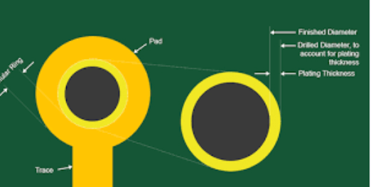
A via is a plated hole in a PCB that connects different layers of the board, allowing electrical signals to pass through. Vias are used to route traces from one layer to another, enabling the creation of complex, multi-layer PCBs. They are essential for high-density interconnect (HDI) designs, where space is at a premium, and efficient routing is critical.
Vias are typically cylindrical in shape and consist of a conductive barrel, which is the plated hole, and pads on the top and bottom layers of the PCB. The barrel is usually filled with a conductive material, such as copper, to ensure a reliable electrical connection. The size and placement of vias are critical factors in PCB design, as they can affect signal integrity, thermal management, and manufacturability.
Types of PCB Vias
There are several types of vias used in PCB design, each with its own unique characteristics and applications. The most common types include:
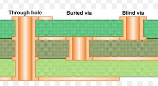
- Through-Hole Vias: These are the most basic and widely used type of vias. They extend through the entire thickness of the PCB, connecting all layers from the top to the bottom. Through-hole vias are relatively easy to manufacture and provide a reliable connection. However, they can take up more space on the board compared to other types of vias, making them less suitable for high-density designs.
- Blind Vias: Blind vias connect an outer layer of the PCB to one or more inner layers but do not extend through the entire board. They are used when it is necessary to route signals from the surface of the board to an inner layer without affecting the opposite side. Blind vias are more complex to manufacture than through-hole vias but offer greater flexibility in routing and can help reduce the overall size of the PCB.
- Buried Vias: Buried vias are entirely contained within the inner layers of the PCB and do not extend to the outer layers. They are used to connect inner layers without affecting the surface layers, allowing for more efficient use of space. Buried vias are more challenging to manufacture than through-hole and blind vias, as they require additional processing steps during PCB fabrication.
- Microvias: Microvias are small vias with a diameter typically less than 150 microns. They are used in high-density interconnect (HDI) PCBs, where space is limited, and fine-pitch components are used. Microvias can be either blind or buried and are often stacked or staggered to create complex routing patterns. Due to their small size, microvias require advanced manufacturing techniques, such as laser drilling, to ensure precision and reliability.
- Via-in-Pad: Via-in-pad is a design technique where a via is placed directly within the pad of a surface-mount component. This approach is used to save space and improve signal integrity by reducing the length of the signal path. However, via-in-pad designs require careful consideration of thermal management, as the via can act as a heat sink, affecting the soldering process.
Design Considerations for PCB Vias
Designing vias in a PCB involves several critical considerations to ensure optimal performance, manufacturability, and reliability. Some of the key factors to consider include:
- Via Size and Aspect Ratio: The size of a via, including its diameter and depth, is a crucial factor in PCB design. The aspect ratio, which is the ratio of the via’s depth to its diameter, affects the manufacturability and reliability of the via. A high aspect ratio can make it difficult to plate the via evenly, leading to potential reliability issues. Generally, a lower aspect ratio is preferred to ensure proper plating and reliable electrical connections.
- Signal Integrity: Vias can introduce impedance discontinuities, signal reflections, and crosstalk, which can degrade signal integrity. To minimize these effects, designers must carefully plan the placement and routing of vias, especially in high-speed and high-frequency circuits. Techniques such as using ground vias, optimizing via placement, and minimizing the number of vias in critical signal paths can help maintain signal integrity.
- Thermal Management: Vias can play a significant role in thermal management by providing a path for heat to dissipate from components to other layers of the PCB or to a heatsink. Thermal vias are often used in high-power applications to improve heat dissipation and prevent overheating. However, designers must balance thermal performance with electrical performance, as excessive use of thermal vias can affect signal integrity.
- Manufacturability: The design of vias must take into account the capabilities and limitations of the PCB manufacturing process. Factors such as the minimum via size, aspect ratio, and spacing between vias must be considered to ensure that the PCB can be manufactured reliably and cost-effectively. Designers should work closely with PCB manufacturers to understand their specific requirements and constraints.
- Cost: The type and number of vias used in a PCB can significantly impact the overall cost of the board. Complex via structures, such as blind and buried vias, require additional processing steps and can increase manufacturing costs. Designers must balance the need for complex routing with the cost implications, especially in high-volume production.
Applications of PCB Vias
Vias are used in a wide range of PCB applications, from simple single-layer boards to complex multi-layer designs. Some of the key applications include:
- High-Density Interconnect (HDI) PCBs: HDI PCBs are used in applications where space is limited, and high component density is required. Microvias and blind/buried vias are commonly used in HDI designs to enable complex routing and reduce the overall size of the board. HDI PCBs are widely used in smartphones, tablets, and other compact electronic devices.
- High-Speed and High-Frequency Circuits: In high-speed and high-frequency circuits, signal integrity is critical. Vias are used to route signals between layers while minimizing signal degradation. Techniques such as via stitching, where multiple vias are used to create a low-impedance path, are often employed to maintain signal integrity in high-speed designs.
- Power Distribution: Vias are used to distribute power and ground connections throughout the PCB. Power vias are often larger in size to handle higher current levels, while ground vias are used to create a low-impedance return path for signals. Proper placement and sizing of power and ground vias are essential for ensuring stable power delivery and minimizing noise.
- Thermal Management: In high-power applications, vias are used to dissipate heat from components to other layers of the PCB or to a heatsink. Thermal vias are often placed directly under high-power components, such as processors or power amplifiers, to improve heat dissipation and prevent overheating.
- RF and Microwave Circuits: In RF and microwave circuits, vias are used to create controlled impedance paths and to connect different layers of the PCB. The design of vias in RF circuits must take into account factors such as via inductance and capacitance, which can affect the performance of the circuit. Techniques such as via shielding and optimized via placement are used to minimize signal loss and interference.
Challenges in PCB Via Design
Despite their importance, vias present several challenges in PCB design. Some of the key challenges include:
- Signal Integrity Issues: Vias can introduce impedance discontinuities, signal reflections, and crosstalk, which can degrade signal integrity. This is particularly problematic in high-speed and high-frequency circuits, where even small discontinuities can have a significant impact on performance. Designers must carefully plan the placement and routing of vias to minimize these effects.
- Manufacturing Complexity: The manufacturing process for vias, especially blind and buried vias, can be complex and require additional processing steps. This can increase the cost and lead time of PCB production. Designers must work closely with manufacturers to ensure that the via design is manufacturable and meets the required specifications.
- Thermal Management: While vias can be used to improve thermal management, they can also introduce thermal challenges. For example, vias can act as thermal bridges, transferring heat from one part of the board to another. This can lead to localized heating and potential reliability issues. Designers must carefully consider the thermal implications of via placement and design.
- Cost: The use of complex via structures, such as blind and buried vias, can increase the cost of PCB production. Designers must balance the need for complex routing with the cost implications, especially in high-volume production. In some cases, alternative design techniques, such as using through-hole vias or optimizing component placement, may be more cost-effective.
- Reliability: The reliability of vias is critical to the overall performance and longevity of the PCB. Factors such as via size, aspect ratio, and plating quality can affect the reliability of the via. Poorly designed or manufactured vias can lead to issues such as open circuits, short circuits, or signal degradation. Designers must ensure that vias are designed and manufactured to meet the required reliability standards.
Conclusion
PCB vias are a fundamental element of modern PCB design, enabling the creation of complex, multi-layer boards with high component density. They play a crucial role in ensuring signal integrity, thermal management, and power distribution, making them essential for a wide range of applications, from consumer electronics to high-speed and high-frequency circuits.
However, designing vias presents several challenges, including signal integrity issues, manufacturing complexity, thermal management, cost, and reliability. Designers must carefully consider these factors when designing vias to ensure optimal performance, manufacturability, and reliability.
As electronic devices continue to evolve, the importance of vias in PCB design will only increase. Advances in manufacturing techniques, such as laser drilling and advanced plating processes, are enabling the creation of smaller, more complex vias, opening up new possibilities for PCB design. By understanding the principles of via design and the challenges associated with their implementation, designers can create PCBs that meet the demands of today’s increasingly complex and compact electronic devices.


