Understanding Schematic Diagrams and PCB Design: A Comprehensive Guide
In the world of electronics, the design and development of printed circuit boards (PCBs) are fundamental to the creation of functional devices. At the heart of this process lies the schematic diagram, a critical tool that bridges the gap between conceptual design and physical implementation. This article delves into the intricacies of schematic diagrams and their relationship with PCB design, exploring their importance, components, and the steps involved in transforming a schematic into a fully functional PCB.
1. Introduction to Schematic Diagrams
A schematic diagram, often referred to as a circuit diagram, is a graphical representation of an electrical circuit. It uses standardized symbols to depict the components of the circuit and their interconnections. Unlike a pictorial diagram, which shows the physical appearance of components, a schematic diagram focuses on the functionality and electrical relationships between components.
Schematic diagrams serve as the blueprint for electronic circuits. They provide a clear and concise way to communicate the design intent, making it easier for engineers, technicians, and other stakeholders to understand and work with the circuit. Whether you’re designing a simple LED flasher or a complex microcontroller-based system, the schematic diagram is the starting point for any PCB design.
2. Key Components of a Schematic Diagram
A schematic diagram consists of several key elements, each of which plays a crucial role in defining the circuit’s behavior. These elements include:
2.1. Symbols
Symbols are the building blocks of a schematic diagram. They represent the various electronic components used in the circuit, such as resistors, capacitors, transistors, integrated circuits (ICs), and connectors. Each symbol is standardized, ensuring that anyone familiar with electronics can interpret the diagram.
For example:
- A resistor is represented by a zigzag line.
- A capacitor is depicted as two parallel lines.
- A transistor is shown as a combination of lines and arrows, indicating its type (NPN or PNP).
2.2. Nets and Connections
Nets are the lines that connect the symbols in a schematic diagram. They represent the electrical connections between components. Nets can be simple, such as a single wire connecting two resistors, or complex, involving multiple branches and junctions.
In schematic diagrams, nets are often labeled to indicate their function or signal type. For example, a net labeled “VCC” typically represents the power supply voltage, while a net labeled “GND” represents the ground connection.
2.3. Power and Ground Symbols
Power and ground symbols are essential in schematic diagrams. They represent the sources of electrical energy and the reference point for voltage measurements, respectively. Common power symbols include “VCC,” “VDD,” and “VSS,” while ground symbols are typically represented by a horizontal line with downward-pointing arrows or a simple triangle.
2.4. Annotations and Labels
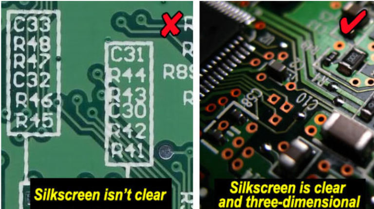
Annotations and labels provide additional information about the components and nets in a schematic diagram. They can include component values (e.g., 10kΩ for a resistor), part numbers, pin names, and signal descriptions. These annotations help clarify the design intent and ensure that the circuit is implemented correctly.
3. The Role of Schematic Diagrams in PCB Design
Schematic diagrams are the foundation of PCB design. They serve as the input for the PCB layout process, guiding the placement of components and the routing of traces on the board. The relationship between schematic diagrams and PCB design can be summarized in the following steps:
3.1. Conceptual Design
The first step in PCB design is to create a conceptual design of the circuit. This involves defining the circuit’s functionality, selecting the appropriate components, and determining how they will be interconnected. The schematic diagram is created during this phase, capturing the design intent in a graphical format.
3.2. Component Selection
Once the schematic diagram is complete, the next step is to select the physical components that will be used in the PCB. This involves choosing components that match the specifications in the schematic, such as resistance values, capacitance, and power ratings. The selected components are then added to a bill of materials (BOM), which serves as a reference for procurement and assembly.
3.3. PCB Layout
The PCB layout process involves translating the schematic diagram into a physical board design. This includes placing the components on the board and routing the electrical connections (traces) between them. The layout must take into account various factors, such as signal integrity, power distribution, and thermal management, to ensure that the PCB functions as intended.
During the layout process, the schematic diagram serves as a reference, ensuring that the connections between components are accurately replicated on the board. Any discrepancies between the schematic and the layout can lead to circuit malfunctions, making it essential to maintain consistency between the two.
3.4. Design Verification
After the PCB layout is complete, the design must be verified to ensure that it meets the requirements specified in the schematic diagram. This involves performing electrical rule checks (ERC) and design rule checks (DRC) to identify any errors or violations. Additionally, simulation tools can be used to analyze the circuit’s behavior and verify its performance before fabrication.
3.5. Fabrication and Assembly
Once the design has been verified, the PCB is ready for fabrication. The fabrication process involves creating the physical board, including the copper traces, vias, and solder mask. After fabrication, the components are assembled onto the board, either through manual soldering or automated assembly processes.
Throughout the fabrication and assembly process, the schematic diagram and PCB layout serve as essential references, ensuring that the final product matches the original design intent.
4. Best Practices for Creating Schematic Diagrams
Creating an effective schematic diagram requires attention to detail and adherence to best practices. The following tips can help ensure that your schematic diagrams are clear, accurate, and easy to interpret:
4.1. Use Standard Symbols
Always use standardized symbols for components in your schematic diagram. This ensures that anyone familiar with electronics can understand the diagram without confusion. If you need to use non-standard symbols, provide a legend or explanation to clarify their meaning.
4.2. Organize the Diagram
A well-organized schematic diagram is easier to read and understand. Group related components together and arrange the diagram in a logical flow, such as from input to output. Use labels and annotations to clarify the function of different sections of the circuit.
4.3. Label Nets and Components
Clearly label all nets and components in the schematic diagram. This includes assigning unique reference designators (e.g., R1, C2, U3) to each component and labeling nets with meaningful names (e.g., “VCC,” “GND,” “CLK”). Proper labeling helps prevent errors during the PCB layout process and makes it easier to troubleshoot the circuit.
4.4. Use Hierarchical Design
For complex circuits, consider using a hierarchical design approach. This involves breaking the circuit into smaller, more manageable subcircuits, each represented by a separate schematic sheet. Hierarchical design makes it easier to manage large designs and allows for better organization and reuse of circuit blocks.
4.5. Perform Regular Reviews
Regularly review your schematic diagram to identify and correct any errors or inconsistencies. This includes checking for missing connections, incorrect component values, and violations of design rules. Peer reviews can also be beneficial, as they provide an additional perspective and help catch issues that may have been overlooked.
5. Common Challenges in Schematic-to-PCB Design
While schematic diagrams are essential for PCB design, the transition from schematic to PCB layout can present several challenges. Some of the most common issues include:
5.1. Component Placement
Proper component placement is critical for ensuring the functionality and manufacturability of the PCB. Components must be placed in a way that minimizes signal interference, reduces thermal stress, and allows for efficient routing of traces. Poor component placement can lead to signal integrity issues, increased manufacturing costs, and reduced reliability.
5.2. Signal Integrity
Signal integrity refers to the quality of the electrical signals as they travel through the PCB. Issues such as crosstalk, reflections, and electromagnetic interference (EMI) can degrade signal integrity, leading to circuit malfunctions. To mitigate these issues, designers must carefully route high-speed signals, use appropriate grounding techniques, and adhere to best practices for PCB layout.
5.3. Power Distribution
Ensuring proper power distribution is another challenge in PCB design. The power supply network must deliver stable and sufficient power to all components on the board. This requires careful planning of power planes, decoupling capacitors, and trace widths to minimize voltage drops and noise.
5.4. Thermal Management
Thermal management is a critical consideration in PCB design, especially for high-power circuits. Components that generate significant heat must be properly cooled to prevent overheating and ensure reliable operation. This may involve the use of heat sinks, thermal vias, and careful placement of components to facilitate heat dissipation.
6. Tools for Schematic Capture and PCB Design
Several software tools are available to assist with schematic capture and PCB design. These tools provide a range of features, from basic schematic drawing to advanced simulation and analysis. Some of the most popular tools include:
6.1. Altium Designer
Altium Designer is a comprehensive PCB design tool that offers advanced features for schematic capture, PCB layout, and design verification. It is widely used in the electronics industry for its powerful capabilities and user-friendly interface.
6.2. KiCad
KiCad is an open-source PCB design tool that provides a complete suite of tools for schematic capture, PCB layout, and 3D visualization. It is a popular choice for hobbyists and small businesses due to its affordability and active community support.
6.3. Eagle
Eagle (Easily Applicable Graphical Layout Editor) is a widely used PCB design tool that offers a range of features for schematic capture and PCB layout. It is known for its ease of use and extensive library of components.
6.4. OrCAD
OrCAD is a professional-grade PCB design tool that offers advanced features for schematic capture, simulation, and PCB layout. It is commonly used in industries such as aerospace, automotive, and telecommunications.
7. Conclusion
Schematic diagrams are the cornerstone of PCB design, providing a clear and concise representation of an electronic circuit. They serve as the blueprint for the PCB layout process, guiding the placement of components and the routing of traces. By adhering to best practices and using the right tools, designers can create effective schematic diagrams that lead to successful PCB designs.
As technology continues to advance, the importance of schematic diagrams and PCB design will only grow. Whether you’re designing a simple circuit or a complex system, understanding the principles of schematic diagrams and their role in PCB design is essential for creating reliable and functional electronic devices.